Astable
Multivibrator using 555
Aim
To simulate an astable multivibrator using IC 555.
Components
|
Name
|
EDWin Components Used |
Description |
Number of components
required |
| RES |
RC05 |
Resistor |
2 |
| CAP |
CAP |
Capacitor |
2 |
| 555 |
LM555 |
Timer |
1 |
| VDC |
VDC |
Dc voltage source |
1 |
| GND |
SPL0 |
Ground |
3 |
Theory

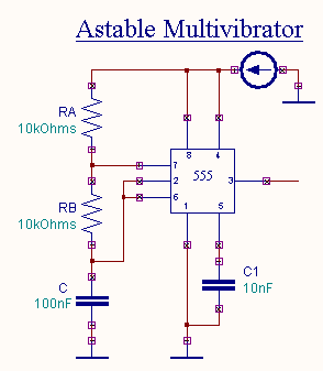
The circuit diagram for the astable multivibrator using IC 555
is shown here. The astable multivibrator generates a square wave, the
period of which is determined by the circuit external to IC 555. The astable
multivibrator does not require any external trigger to change the state of the output. Hence the name free running oscillator.
The time during which the output is either high or low is determined by
the two resistors and a capacitor which are externally connected to
the 555 timer.
The above figure shows the 555 timer connected as an astable
multivibrator. Initially when the output is high capacitor C starts charging
towards
Vcc
through RA and RB.

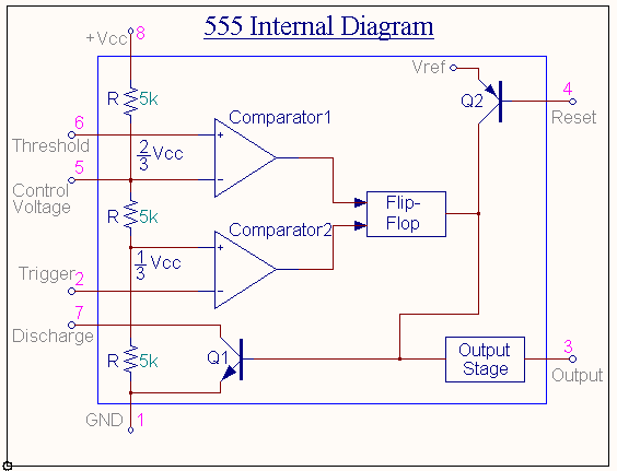
However as soon as the voltage across the capacitor equals 2/3 Vcc
, comparator1 triggers the
flip-flop and the output switches to low state. Now capacitor C
discharges through RB and the transistor Q1. When voltage across C
equals 1/3 Vcc, comparator
2’s output triggers the flip- flop and the output goes high. Then the cycle
repeats. The capacitor is periodically charged and discharged between 2/3 Vcc
and 1/3 Vcc respectively.
The time during which the capacitor
charges from 1/3 Vcc to 2/3 Vcc is equal to
the time the output remains high and is given by
tc=0.693(RA+RB)C
where RA and RB are in ohms and C
is in Farads. Similarly the time during which the capacitor discharges from 2/3 Vcc
to 1/3 Vcc is equal to the time the output is low and is given by
td=0.693RBC
Thus the total time period of the output waveform is
T=tc + td=0.693(RA+2RB)C
Therefore the frequency of oscillation 
The output frequency, f is independent of the supply voltage Vcc.
Procedure
EDWinXP -> Schematic Editor: The
circuit diagram is drawn by loading components from the library.
Wiring and proper net assignment has been made. Values are assigned.

for relevant components.
EDWinXP-> Mixed Mode Simulator:
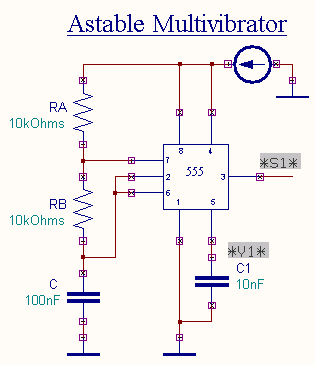
The circuit is preprocessed. The waveform marker is placed at the output
of the circuit. GND net is set as the reference net. The Transient Analysis parameters are also
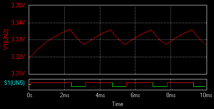
set and the Transient Analysis is executed. The output waveform is
observed in the Waveform Viewer.
Result
The output waveform may be observed in the waveform viewer.
