Positive Negative and Biased Clamper
Aim
To simulate a clamper circuit.
Components
|
Name
|
EDWin Components Used |
Description |
Number of components
required |
| CAPACITOR |
CAP |
Capacitor |
1 |
| RES |
RC05 |
Resistor |
1 |
| DIODE |
1N4007 |
Diode |
1 |
| VGEN |
VGEN |
Ac voltage source |
1 |
| VDC |
VDC |
Dc voltage source |
1 |
Theory
Clamper is a circuit that "clamps" a signal to a different dc level. The different types of clampers are positive, negative and biased clampers.
A clamping network must have a capacitor, a diode and a resistive element. The magnitude R and
C must be chosen such that the time constant RC is large enough to ensure that the voltage across the capacitor does not discharge significantly during the
interval the diode is non- conducting.
Positive Clamper
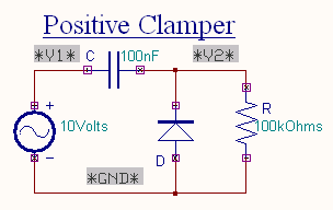
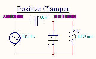
The circuit for a positive clamper is shown in the figure.
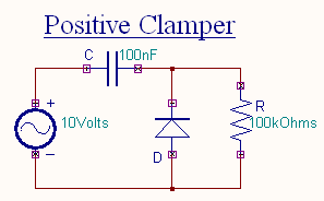
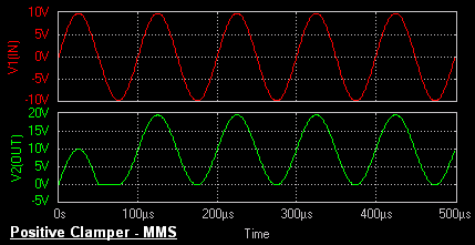
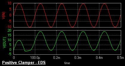
During the negative half cycle of the input signal, the diode conducts and acts like a short circuit.The output voltage Vo = 0V . The capacitor is
charged to the peak value of input voltage Vm. and it behaves like a battery. During positive half of the input signal, the
diode does not conduct and acts as an open circuit.
Hence the output voltage Vo = Vm + Vm This gives a positively clamped voltage.
Negative Clamper
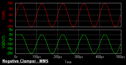
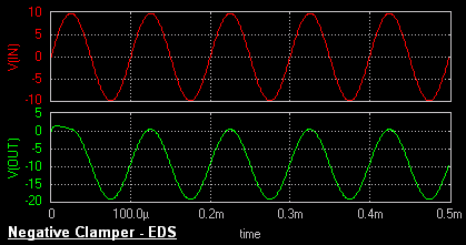
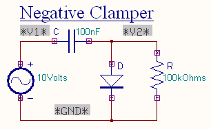
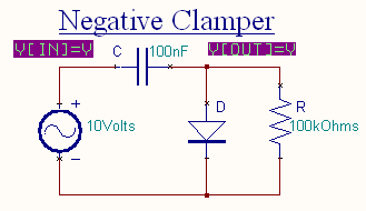
During the positive half cycle the diode conducts and acts like a short circuit. The capacitor charges to peak value of input voltage Vm
. During this interval the output Vo which is taken across the short circuit will be zero.
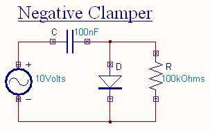
During the negative half cycle, the diode is open. The output voltage
can be found by applying KVL.


Biased Clamper
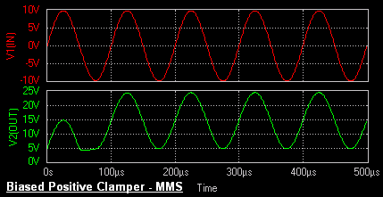
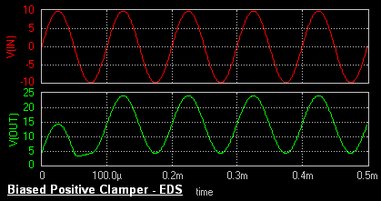
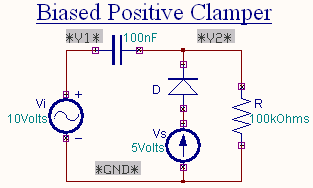
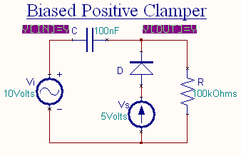
The circuit of a positively biased clamper is shown in the figure. During the negative half cycle of the input signal
the diode is forward biased and acts like a short circuit. The capacitor charges to Vi + Vs . Applying the KVL
to the input side


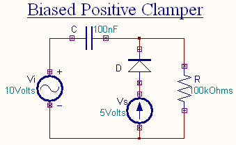
The voltage across the resistor will be equal to the source voltage Vs .
During the positive half cycle of the input signal, the diode is
reverse biased and it acts as an open circuit. Hence Vs
has no effect on Vo.
Applying KVL around the outside
loop.


Procedure
EDWinXP-> Schematic Editor: The circuit diagram is drawn by loading components from the library. Wiring and proper
net assignment has been made. The values are assigned for relevant components.
EDWinXP -> Mixed Mode Simulator:
The circuit is preprocessed.
The test points and waveform
markers are placed in input and output of the circuit. GND net is set as
reference net. The Transient Analysis parameters have been set.
The Transient Analysis is executed and output waveform is observed in
Waveform Viewer.
EDWinXP -> EDSpice Simulator: The circuit is preprocessed. The test points and waveform
markers are placed at the input and output of the circuit. The instance
parameter for components and Transient Analysis parameters have been set.
The Transient Analysis is executed and output waveform is observed in
Waveform Viewer.
Result
The output waveform may be observed in the waveform viewer.
