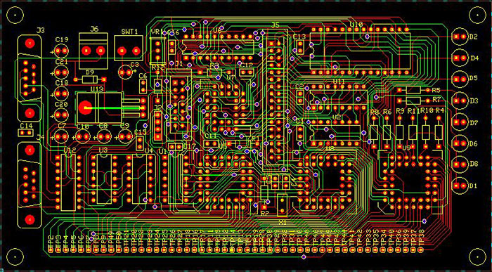
LAYOUT EDITOR
Layout Editor is used to design the PCB layout of a circuit. The design can be captured either in
Schematic Capture or directly in Layout Editor. In the former case, the design is
Front Annotated to
the Layout Editor and in the latter case it is Back Annotated to Schematic Editor. Also allows beginning
layout without a preexisting schematic. In layout the components are placed using Library
Browser or
Library Explorer. Each of the components placed is labeled which displays information about the package.
The component pins are connected using Trace or Nets.

Automatic operations like DRC Check, Renumbering of Components, Placing Components and Routing is also possible
from within this editor.The components may be autorouted using Arizona autorouter, which is an integrated module of
EDWin XP/2000.
SPECCTRA Translator supports different options like Converting EDWin XP/2000 Project (database) to SPECCTRA
Compatible Format, Importing Results from SPECCTRA Autorouter and Autoplacer
etc. MaxRoute Translator allows
to convert EDWin XP/2000 layout project (database) to a form that is acceptable to
MaxRoute Autorouter and MaxRoute
Autoplacer. Once when a design is complete, necessary notes may be added by selecting appropriate tools. This Editor
also allows editing Already Existing Projects.
Board design and board analysis Overview
Other by auto router wiring, performs the wiring with rip-up function, you can output such as Gerber / drill data and parts center coordinate data of the substrate. The equipment of tools such as parts and auto-layout and fan-out analysis and wiring density display, solid surface and teardrop automatic generation · 3D viewer, can be more complete board design.
In input use of mechanical CAD output outline DXF data, substrates of complex shapes, can be easy layout.
3D viewer of standard equipment, can be confirmed from each direction in a three-dimensional, including the housing not only the substrate, also available in the document.
The Plus Pack, included with the board thermal analysis to check the temperature of the environment. Plus + in the pack, I have added the electromagnetic field analysis and signal degradation analysis that enables a more detailed board simulation.
Main function
- Automatic component placement
- Semi-automatic wiring with auto-router correction function
- With rip-up wiring function
- Circuit symbol / pin number automatic re-allocation
- Block editing
- Part shape reference browser display
- Hole layout display
- Solid surface connection check
- Board outline DXF data input
- DXF output
- Bitmap graphic placement, such as logo
- Board placement of Japanese fonts
New features what has been strengthened
-
Stepless scroll scaling display
- Real-time bi-directional block copy pasting
- Automatic arc Smoothing wiring
- Partial taper wiring
- Wiring length / width specified wiring generation
- Impedance calculation function with wiring
- DRC check with automatic wiring correction
- Back wiring table pad blind via automatic generation
Real-time bi-directional block copy pasting
Copying attaching a schematic block, with the exception of the net which is not connected in a block, immediately is reflected in the layout. Similarly, when a layout block to copy pasting, it is reflected in the circuit diagram.
Pair wiring automatic parallel arrangement
Since such anti-noise and impedance matching, if necessary parallel pair wiring arrangement, by specifying the net connection destination to specify wiring criteria for each start pad pair wiring, and parallel up to 8 wires You can automatic placement.
Connection destination of each net other than the reference net I can be connected by a drag operation.

Selection of designated wiring standard net of each start pad to pair wiring

Drag operation connection of net other than the reference net
Automatic arc Smoothing wiring
And by a smooth arc wire, issues a high frequency portion of the wiring and the wiring density is reduced.
Partial taper wiring
Was partially or narrow or wide the wiring width, current measures and wiring density, etc., to improve the degree of freedom in design.
Wiring length / width specified wiring students
By the setting of partially wiring length / width, you can generate the wiring that was the rule of.
Check the resistance-capacitance-Indatansu impedance after wiring, it is also possible to modify.
Impedance calculation function with wiring
The layer structure is designed, and assigned the layer type (PWR / GND, signal or mixed), the conductor layer thickness, by setting a such as an insulating layer thickness and parameters, can be automatic generation of impedance of stripline and microstrip wiring that desire is.
Back wiring table pad blind via automatic generation
I want to facilitate the wiring to the SMT components.
For board design tools included
Autorouter
The auto-router that exert an effect on the logic system wiring, I have been standard equipment.
DRC check
DRC check, between the pads between the pattern pad - Check the inter-trace.
Based on the set design rules, do the automatic correction of the defective part.
Fan-out configuration
Set the current capacity of each net, can be wired in the optimum pattern width.
Teardrop automatic generation tool
It will automatically generate a teardrop to increase the pad strength.
Know More about Layout Editor