8051-RAM-Write-Read
This 8051 project shows the memory read and write operation. To simulate circuit in this project, initially activate Mixed Mode simulator from the Schematic Editor window. Simulation can be performed by selecting Run Transient analysis / Oscillograph from Simulation menu.
The circuit contains an 8051 chip, Dual Positive Edge Triggered D Flip-Flop with preset and clear (7474), 2 Input Positive AND Gate (7408), Quad 2-Line to 1-Line Data Selectors/Multiplexers (74157), 8K x 8 Bit Fast Static RAM (MCM6264C), 2 Input Positive NOR Gate (7432), Hex Inverter (7404), Synchronous 4-Bit Up/Down Counter with Mode Control (74191), 7-Segment Decoder/Driver/Latch (9368) and Bus Transceiver With 3-State Output (74LS245).
Component Description:
Bus Transceiver With 3-State Output (74LS245).
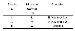
These octal bus transceivers are designed for asynchronous two-way communication between data buses. The control function implementation minimizes external timing requirements. The device allows data transmission from bus A to bus B or from bus B to bus A depending upon the logic level at the direction control (DIR) input. The enable control input (G) can be used to disable the device so that the buses are effectively isolated.

7-Segment Decoder/Driver/Latch with Constant Current Source Outputs (9368)
The 9368 is a 7-segment decoder driver designed to drive 7-segment common cathode LED displays. This drives any common cathode LED display rated at a nominal 20 mA at 1.7V per segment without need for current limiting resistors. This device accepts a 4-bit binary code and produces output drive to the appropriate segments of the 7-segment display. It has a hexadecimal decode format, which produces numeric codes ‘0 ‘to ‘9’, and alpha codes ‘A’ to ‘F’ using upper and lower case fonts.
Operation

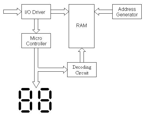
During WRITE operation, both 74245 drivers will be working in A data -to-B bus mode. Microcontroller together with decoding circuit generates the necessary control signals from the RAM. The counters, (74191) are cascaded together and save the purpose of address generation. After the completion of one WRITE cycle, the INT0 pin of Microcontroller is enabled, which is generated by the counter 74191.This completes the WRITE process.
After the WRITE operation, first 74245 is buffered to ‘Z’ state and the second 74245 works in B data-to-A bus mode. Microcontroller together with decoding circuit generates the necessary control signals from the RAM. Microcontroller reads the data from the RAM through the second 74245 and displayed in the
7-segment form
through the driver. The READ operation may be repeated.
The program is as shown:
#include <8051.h>
void myint_t0() interrupt 0;
void delay (int Time);
void main ()
{
int i=0; // Variable I is initialized with value ‘0’.
int k; // Variable k is declared
EA =1; // EA is set to enable all interrupts
EX0 = 1; // EX0 is set to enable external interrupt 0
P0_0 = 1; // P0.0 is set to value ‘1’
P0_1 = 0; // P0.1 is set to value ‘0’
P0_2 = 1; // P0.2 is set to value ‘1’
P0_3 = 0; // P0.3 is set to value ‘0’
P0_4 = 1; // P0.4 is set to value ‘1’
for( ; ;) // Infinite loop
{
k= P1; // Value at Port P1 is copied to variable k
P2 = k; // k is copied to Port P2
}
}
void myint_t0() interrupt 0
{
P0_0 = 0; // P0.0 is set to value ‘0’
P0_1 = 1; // P0.1 is set to value ‘1’
P0_2 = 0; // P0.2 is set to value ‘0’
P0_3 = 1; // P0.3 is set to value ‘1’
P0_4 = 0; // P0.4 is set to value ‘0’
delay (50);
P0_3 = 0; // P0.3 is set to value ‘0’
P0_0 = 1; // P0.0 is set to value ‘1’
}
void delay(int Time) // Delay function description
{
while (Time)
{
Time--;
}
}
The source code in the
code editor window
has to be
compiled
after making any modifications
(editing).
Also the code can be
debugged
during
simulation.