Multi Layer Routing in EDWinXP
Multilayer PCBs are widely used in various electronics devices with number of advantages such as high assembly density, small size, good quality, reliability, good quality,
good quality and so on. In addition, multilayer PCBs offer superior reductions in distortion and signal propagation
in applications where signal integrity and
“cross talk” levels are critical. However the initial costs of Multilayer PCBs are higher than that of Single Sided or Double Sided PCBs.
Their benefits are extensive and they have revolutionized the electronics industry and defined the future of printed circuit board as a whole.

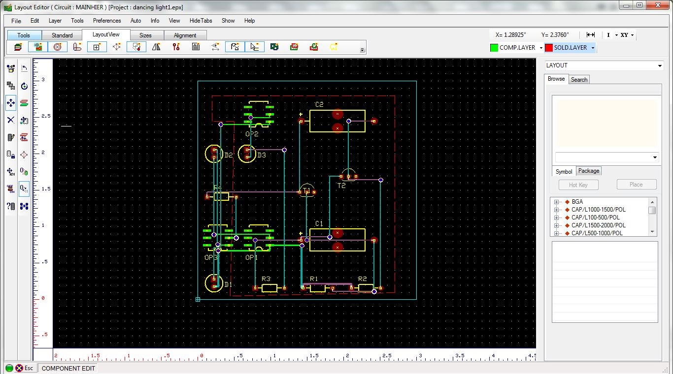
In single layer, we can see the circuit like the below

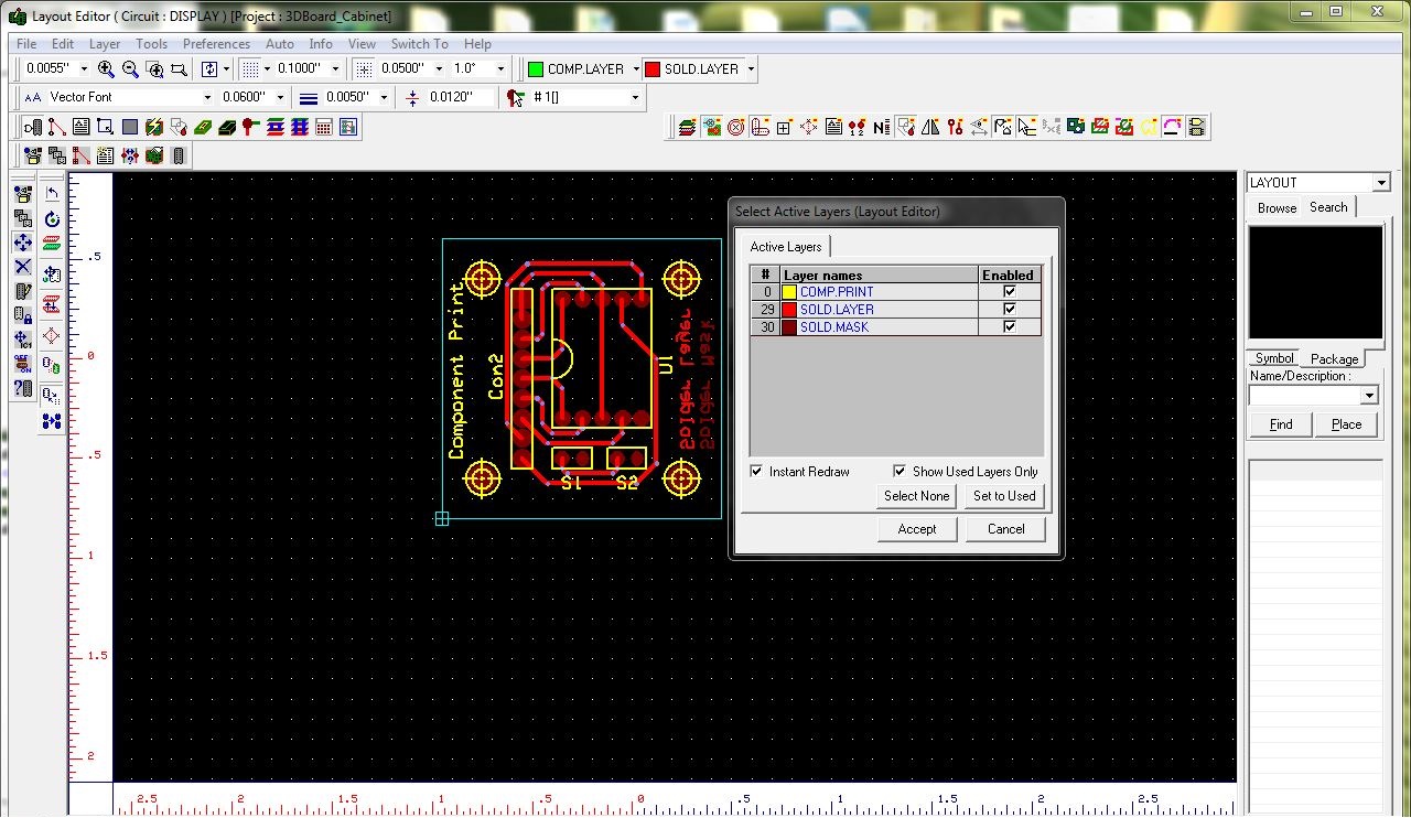
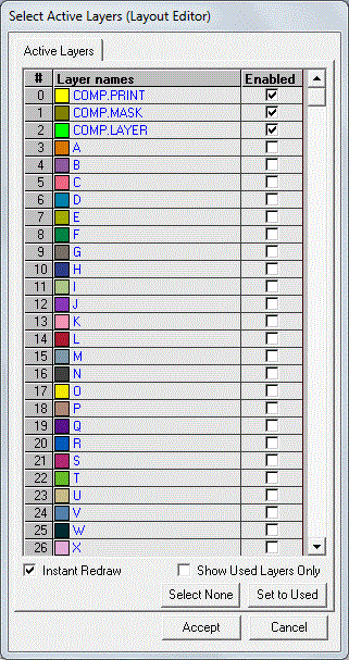
To select multilayer routing in Layout Editor of EDWinXP, select Active layers

.
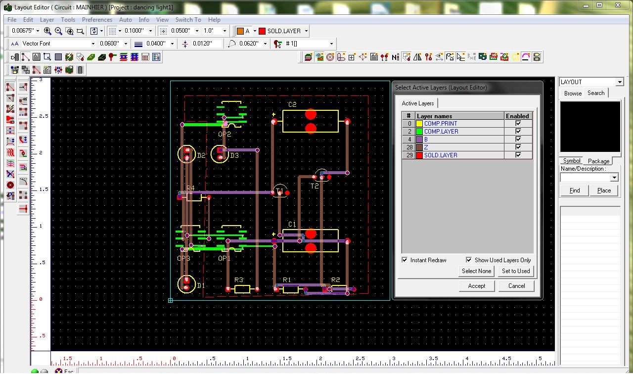
This option is used in complex projects to easily identify the different connections in the ciruit.

