A. Design circuit using Schematic Editor
1. Loading the Component2. Packaging the Component
3. Routing the wire connections
4. Entering Page and Design Notes
5. Saving the Project
6. Printing the Schematic diagram
B. Creating PCBs using PCB Layout
1. Drawing Board outline
2. Placing the Components
- Manual placement
- Automatic Placement
3. Routing Components
- Manual Routing
- Semi Automatic Routing
- Autorouting
o Autoroute Trace
o Specctra Autorouter
o MaxRoute Translator4. Creating copper pour graphic items
5. Testing the Board
1. Connectivity Test
2. Design Rule Check
3. Copper pour flood test
C. Creating Gerber using Fabrication Manager
1. GERBER Output
2. Gerber Output Parameters
3. Define Layers and Generate GERBER Output
4. Preview the GERBER Data
5. Add Notes to GBR Files
6. Introduction to NC Drill
7. NC Drill Output Parameters
8. Generate NC-Drill Data
9. Introduction to PCB Assembly outputs
10. Introduction to Bare Board Testing outputs
Schematic Editor
Invoke Schematic Editor from Project Explorer in the following ways.
Right click Page [Main Page] and Select Edit Page from the list.
Select Edit Page from the task list or from the task toolbar.
• Turn ON Grid by enabling the grid from the dropdown, in Standard Toolbar.
• The value for grid may be selected from the drop down list as .1000”.
• Set Snap value to .0500” for better placement of the components.
Loading the Components
Select Tools → Components toolbar and right click on the workspace to popup a set of Component editing tools. By default, relocate tool is enabled.
Note: Create library (symbol, Package and part) of necessary components(part
list) before starting schematic design.
Loading Components using Component Browser
• The component browser is launched from View → Schematic → Browser.
• The required components can be obtained either by using the Browse option in the window or by Search for the element in the quick menu
• Using the Place button in the bin we can place the components in the workspace.
Note:
Hotkeys can also be assigned to element names by which quick launch of components
is possible.
Battery and Ground can be obtained from the Component Browser. These are external sources (which will not be housed on the PCB) and hence connections to them can be shown with the help of connectors. Select connectors from the component browser, then select List Connector and select the required header from the list appearing Load the connector and using Repeat Component function tool, create the required number of instances. Similarly load SPL0 (Hotkey G).
To relocate the component, right click and select tool Relocate. Position the part where required and click the mouse to place component
Note: Auto placer can be used to place component automatically.
Packaging the Components
If the PCB of the circuit has to be designed, then the components need to be packaged. Packaging is nothing but information that the system requires identifying the Package associated to Part placed on the Schematic. Only packaged components are automatically front annotated to layout.
Interactive Packaging
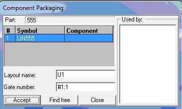
Interactive packaging is done using the tool Pack/ Unpack Component. Right click and select this tool and click on the component pin that is to be packed. A window “Component Packaging” pops up. Click Accept button. This method allows individual packaging of components.
Routing the wire connections
Connections between components are established using WIRES and BUSES.
1. Select Tools → Connections to enable a set of tools required for routing.
Tip: Adjust zoom precision
to view the terminals being wired. Turn ON grid and snap to help in positioning
the wires.
2. Before creating the connections, enable Preferences → Instant net name and Preferences → Instant wire label.
3. Right click on the work space and select Connections.
4. Enable Pin to Pin option tool whenever an entry or pin is clicked for making a connection. This ensures that the connection is made to the pin.
5. An input box appears prompting the user to enter the name of the net, enter the name most suited for the net.
Entering Page Notes and Design Notes
Page notes appear only on the current page (e.g. Page No.) of the project whereas Design notes appear on all the pages (e.g. Project name) of the selected circuit.
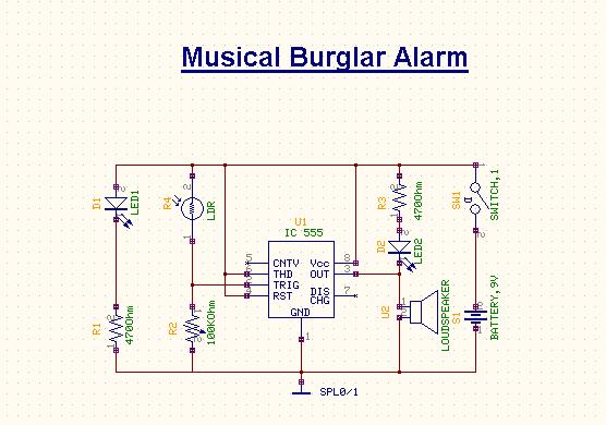
1. Select Tools → Page Notes toolbar to enable a set of tools for creating page notes. Right click and enable
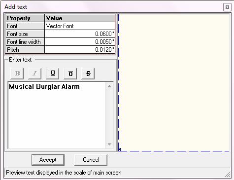
2. Create PN Graphic Item tool → Create Text to open a window Add Text block. Enter the required notes and accept it.The text gets tagged to the cursor. Now place the text at desired position. To edit this text, Press Ctrl key and click on the text to select it. Perform the various operations using bullets.
Saving the Project
In order to prevent loss of work, save the project periodically using the following steps.
1. On the File menu of Project Explorer, Click Save Project or Press Ctrl + S.
2. The first time Save Project is selected, a dialog pops up prompting to enter the name for the project.
3. Type in the name of project as Musical Burglar Alarm.epb
Printing the Schematic Diagram
To print the Schematic diagram, select File/ Print page from the main menu of Schematic Editor. A window pops up with the preview of circuit diagram. Click on ‘Fit graphic to one page with margin’ icon. Click on Print Page icon to print the page.
PCB LAYOUT
PCB Layout is invoked from Project Explorer in the following ways.
• Right click PCB Layout and select Edit PCB Layout from the list.
• Select Edit PCB Layout from the task list or from the task toolbar.
Steps to follow to define board outline
i. Select Tools → Board Outline
ii. Select Define Outline (function tool) → Create Board (option tool). This tool enables free hand drawing, using which a board of desired shape can be drawn on the workspace.
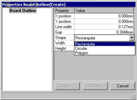
iii. To select a pre-defined board format, select the option tool Textual Mode. The Properties Board Outline (Create) dialog pops up.
iv. Enter the desired values and click Accept button.
Choose Layer
Choose required layer (comp.layer) for placing components
Relocating the components
The components placed on the schematic, which contain both symbol and package, are front annotated to the layout after packaging. These components are positioned at board datum (0,0) automatically and may be relocated either manually or automatically
Note: Only parts that contain both symbol and package will be automatically
back annotated to the schematic. Auto placer can be used to place component
automatically within the board.
Before we start loading Parts on to the page, turn ON Grid by enabling grid from the dropdown, in Standard Toolbar. The value for grid may be selected from the drop down list as .1000”.
Similarly, set Snap value to .0500” for better placement of the components.
Select Tools → Components → Relocate Component (funtion tool) to relocate the components.
Enable Ratsnet (F7 key) option tool of Relocate Component function tool to view ratsnest while relocating the components to ensure that components having a large number of interconnections are positioned close to each other. Pressing SHIFT key while relocating/ stretching an item allows the item to move/ stretch smoothly.
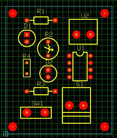
Note: The silkscreen reference designator is relocated
outside the component body after the part placement is completed
Routing the Components
Connections between components may be established by using Traces and Copper Pour areas.
1.Make sure you've set the track thicknesses as you want before routing or set it in Project Explorer, select Project / Project Design Rules and set the routing width to 0.030” for Pwr/Gnd lines and 0.013” for Signal lines.
2. Select auto routing for routing board automatically or rout the board manually as well.
Manual routing
1. Select Tools → Connections → Route (Function tool) to enable a set of Routing tools on right clicking the workspace.
Tips:
• Adjust zoom precision to view the pins properly.
• Turn on Preference/ Guidelines (Next unconnected node) before routing because this option guides you to take the easiest path to route.
• Select True Size and Pad frames from View/ Layout, enabling you to select proper trace size. This also prevents you from creating errors such as traces crossing over pad, traces very close together etc.
Route power and ground first, especially if it's a 1 or 2 layer board. Or you can copper pour GND signal in multilayer board which allows creation of large ground (and/or power) areas .This improves noise properties. Also reduces amount of copper that needs to be etched off the board by manufacturing process,
To start routing traces, first select the critical nets;
• The trace connection may now be created in the following way.
1. Select layer for routing from Layers in the main menu. 28 layers are available for routing. By default COMP LAYER is selected. Click on pin to route on SOLD LAYER.
2. Tips: While routing, enable the tool Snap Trace by 45 degree to change routing directions in steps of 45 deg only.
3. Move cursor with 45° angle through a short distance and click at the nearest point.
4. Terminate routing of the trace by pressing END or F4 key on your keyboard. Or click on the tool End Connections.
Auto Routers
Allows routing the current Project automatically by selecting any one of the three autorouters available.
• Autorouter - Arizona
• Autorouter - Specctra
• Autorouter - Maxroute
Arizona Autorouter
Arizona auto router is an integrated module of the EDWinXP. It uses its own temporary project and simplified graphics. The Arizona auto router allows routing the traces of a PCB Layout automatically.
Autorouting using Arizona Auto router
1. Select Auto → Auto Router → Arizona.
2. Select File → Load board to route from project.
3. Select Parameters Setup (function tool) → Routing Parameter Settings (option tool).
4. Check Solder Layer in the Routing Parameters Settings windows.
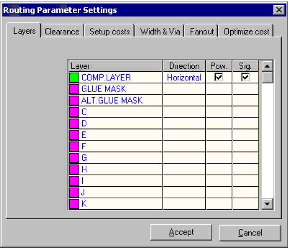
5. Select Auto routing Routines (function tool) → Start Auto Router.
6. Select Auto routing Routines → Miter.
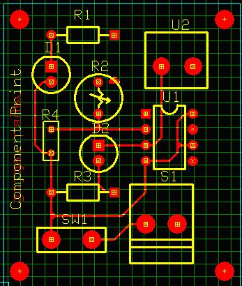
7. Close Arizona Auto router window, Click Update project and Exit to save the project
Copper Pouring
Select Tools → Copper toolbar to enable a set of tools for creating Copper pour. Right click and enable
1. Select Create copper graphic item function tool and Create copper pour area from option tool
2. Select the layer(eg: Layer Y)where the copper pouring is to be done and select the net SPL0 in sizes toolbar
3. Draw copper pour in required area
4. Enables Meshed copper pour area in Preferences tools to enable meshed View of copper pour.
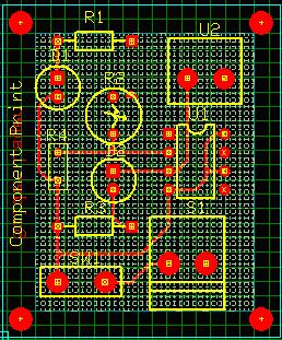
Testing the Board
While designing a PCB, it is quite obvious that a number of errors may occur. These errors may be in the form of overlapping pads, unconnected Nodes, traces crossing another trace, etc. Such errors must be taken care of before printing the PCB. To find out such errors, certain checks on the board are done. Connectivity and DRC check are the two checks.
Connectivity Test
Connectivity test may be used to check whether there is any electrical discontinuity (unconnected nodes or deleted trace segments) in a single net. By setting certain parameters, the test can be performed either on individual nets or all the selected nets.
i. Select Tools → Connections → Connection Property → Test Connectivity
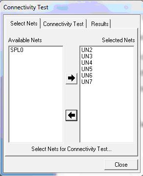
ii.Click on the board or on a net. The Connectivity Test dialog pops up.
iii. Select the required nets using the move keys and click the connectivity test tab.
iv. Select Connectivity test tab, set anyone of the three options:
- Stop at first fail: Test stops at the first occurrence of error.
- Test all selected Nets: Checks whether all NODES of the selected NETS are connected.
- Test single Net: Checks connectivity of the NODES of the selected NET.
v. Click the Test button to display the results.
vi. Perform this test until “Tested Nets – Fully Connected” message is displayed in this window.
Design Rule Check (DRC)
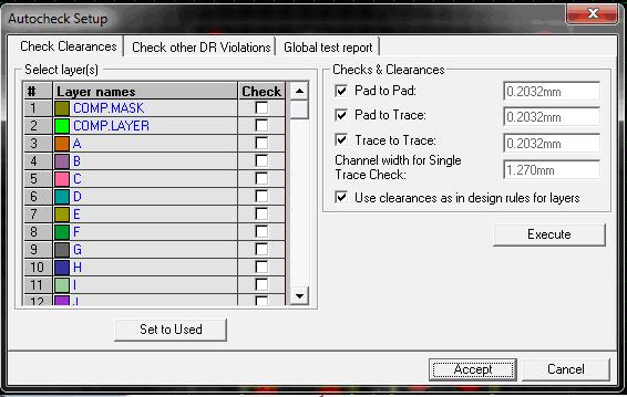
This utility is used to create an error free board to enhance the efficiency of your board. It automatically smoothes, miters, and checks for both aesthetic and manufacturing problems that might have been created in the process of manual or automatic routing. This test helps us to check the clearance between pad to pad, pad to trace and trace to trace.
i. Select Autocheck from Auto Menu. The Clearance Check dialog pops up.
Select the layers and enter the clearance value in the window. To select all the layers used in the project click the SET TO USED button.ii. Click Execute
Copper pour flood test
This check finds out isolated pockets of copper and detects pads that were cut off. It is needed in Editor for previewing how result of component placement and routing within copper pour will look on artworks. Additionally, it provides a way to present air gaps graphically. In another words, flood test has generally the same purpose as in Fabrication Manager and works in somewhat similar way.
Operation
1. Select Tools → Connections → Connection
property tool → Copper
pour flood test . Activate this option and then click on the copper pour
area. A new window appears as shown in figure below.
The user can select the test from the drop down menu of Select Test.
The test starts by pointing flooding point within boundaries of copper pour
polygon.
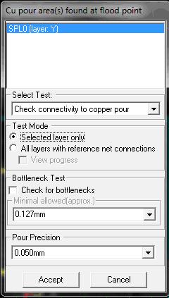
The display presenting flooded areas (red), isolated (black) and air gaps (white) with superimposed layer over it, stays put until ‘Esc’ or until next polygon selection. (The same Copper pour flood test has been added as option to Copper → Copper item property tool) .Which of copper pour areas will be tested depends on flood point position. Program establishes all other parameters automatically. In cases when few polygons on different layers overlap at flooding point, there is a possibility provided to select net and flooding layer. Flooding may be applied to current layer where selected polygon resides or to all layers where there are connections for tested net. The test checks always for bottlenecks in the same way as in Fabrication manager. However, it takes always currently set value of trace width as minimal allowed bottleneck.
Fabrication Manager
Fabrication is the last stage of the electronic design process. The PCB information is converted into ASCII output files – GERBER (.gbr), NC Drill (.ncd), PCB Assembly Outputs Generic (.pck), IPC-D-355(.355), Bare Board Testing Generic (.bbt) and IPC-D-356A(.356) which are input to machines to finally create the hardware.
1. Invoke PCB Layout in the Project Explorer.
2. Select Fabrication Manager from the tasklist or Select from the task toolbar. The Fabrication Manager window opens with a default board size and gets aligned with the Project Explorer to fit the screen.
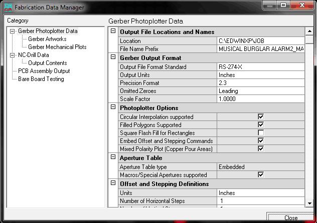
3. Invoke Fabrication Data Manager choose Setup from Fabrication.

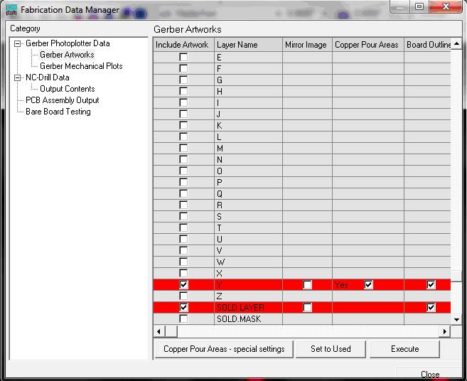
4.Choose Gerber Artworks in the left pane of Fabrication Data Manager .
Gerber Output
GERBER is the standard format used as input to photoplotters that generate the design data on films. These films are used as masters for manufacturing the PCB, the physical realization of the schematic data. GERBER format is a vector format for defining various elements of the layout. This format represents all traces as draw and the pads that are part of the component footprint as flashes. The Photoplotter uses this command language
1. Select the layers for which we want the Gerber Artwork files.
2. Click Execute.
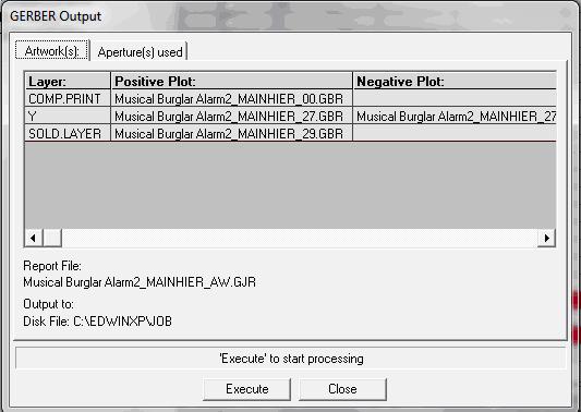
3. ‘Gerber output window’ opens, Click on Execute.
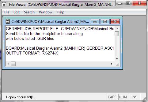
This completes the generation of GERBER data.
Viewing Artwork
1. 1. Invoke PCB Layout in the Project Explorer.
2. Select Fabrication Manager from the tasklist
3.Select Artwork from tools
“Select Layers for Preview” window popping up
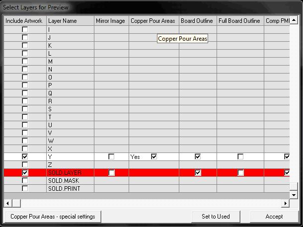
Click on Set to used and Accept button to view art work
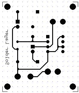
The Artwork of a PCB is the actual display of the various copper routes, padstack, pinholes, etc.. The design data may be viewed layer by layer as it is got on the photoplotted film or pen plotted artwork. This menu option must be active to view the various layers of the design individually.
4. Select Centreholes from View → Artwork → Centreholes as 1/3 Size.
5. In order to view layers, Select view → Toolbar → Layers
( Comp.side & Sold.side) drop down menu and select the required layer. The artwork for that particular layer may be viewed as it appears. Select Solder Layer from tool bar
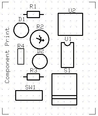
Gerber Mechanical Plots
This window allows setting the parameters for gerber mechanical plots on both Component and Solder side. The window opens with the Component Side, by default. Here the Generate Mechanical Plot for Component Side checkbox is unchecked. Enabling this checkbox displays the list of parameters that may be set.
1. Select Fabrication → Setup. This dialog box is shown below.
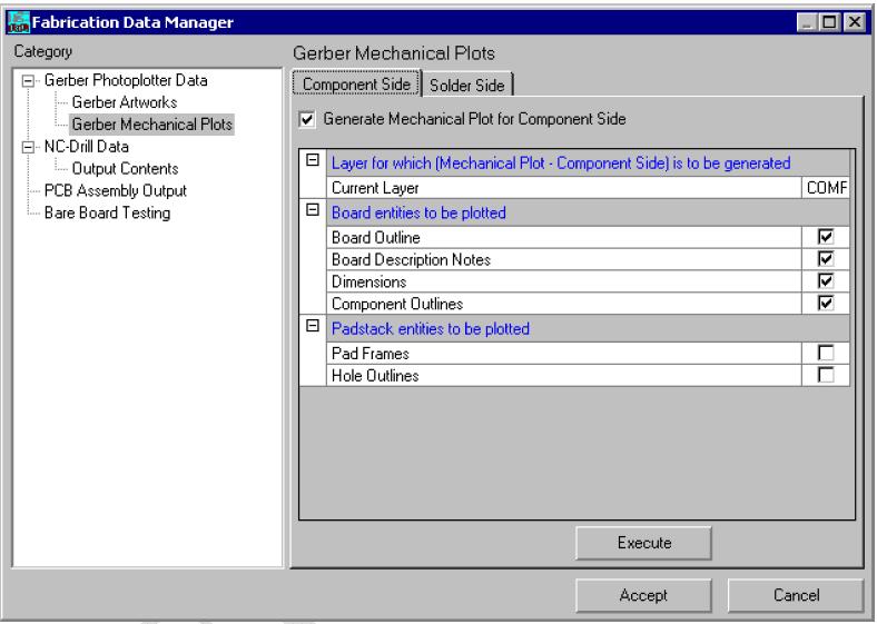
Click Execute, then a Gerber Output window appears.
2. Click Execute. ‘Gerber ASCII output completed’ message appears in the bottom of the window. The output obtained will be a text file.
Introduction to NC Drill
In generating the NC-Drill, the system extracts information about the whole positions, sorts them according to drill size information. The different hole sizes are grouped together and generally sorted to drill in a specific order. This grouping may be done based on sizes, type of drilled hole, like through plated or non-plated, via type like buried or unburied etc. This is generated as a drill tape data. The data may be used directly on any numerically controlled drilling machine. This NC-Drill data is of the EXCELLON format, which is the accepted industry standard.
NC Drill Output Parameters
Select Fabrication → Setup → Fabrication data manager → NC-Drill Data. Depending on the equipment used by the PCB manufacturer some parameters must be set prior to generation of NC drill files.
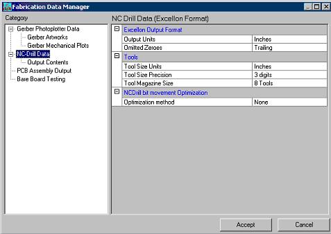
Set the following parameters
Output units - inches or millimeters.
Omitted Zeroes: Leading or Trailing.
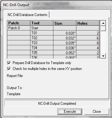
1. Click on Execute, NC Drill Output window appears.
2. In this window check Prepare drill database for Template only and Check for multiple holes in the same XY position.
3. Click on Execute. In this window after execution displays a message ‘NC Drill Output Completed’.
4. Click Close and Accept Fabrication Data Manage.
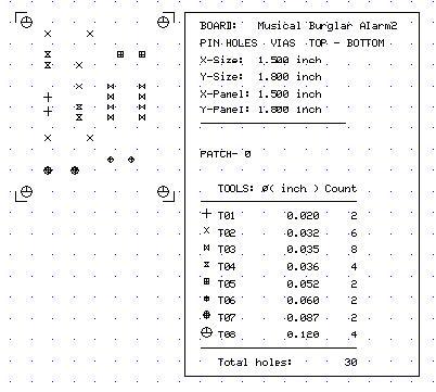
Preview NC- Drill data:
Select Tools → Template(notes)
Generate PCB Assembly outputs.
1. Select Fabrication → Setup → PCB Assembly Output.
2. Click on Execute.Output is a extension .PCK extension file.
3. Save it
4. Select IPC-D-355 tab on top of the Fabrication Data Manager window.
5. Click on Execute. Output is a .355 extension file, save it in the desired location.

Introduction to Bare Board Testing outputs
Bare Board Test (BBT) is like quality check usually done by the fabricator to check the open & short circuits in and between the tracks. A supply of 50 volts is passed through the tracks and this job is done by automated machines. A probe sort of thing is inserted through the pads so as to probe. A netlist is generated from the gerber (it is not generated from the design) so that to cross check the actual physical PCB manufactured with respect to actual gerber in order to find out the fabrication errors.This is a special on board test outputs generated in Generic and IPC-D-356A.
Generate Bare Board Test outputs
Select Fabrication → Setup. To setup parameters for Bare Board outputs choose Bare Board Testing node from Fabrication data manager Choose either format and set the required parameters. Click EXECUTE to generate the Bare Board Testing output in either Generic or IPC-D-356A format.
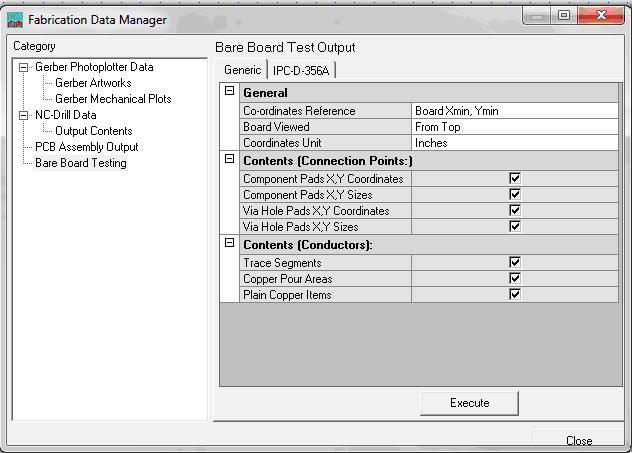
The output for Bare Board Testing is obtained as a text file.