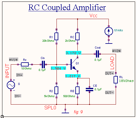
RC Coupled Amplifier
Aim
To design and simulate a RC Coupled Amplifier circuit.
Components
Name |
EDWin Components Used |
Description |
Number of components required |
| BC107 | BC107A | Transistor | 1 |
| RES | RC05 | Resistor | 6 |
| CAP | CASE-A600 | Capacitor | 3 |
| VGEN | VGEN | Ac voltage source | 1 |
| VDC | VDC | Dc voltage source | 1 |
| GND | SPL0 | Ground | 2 |
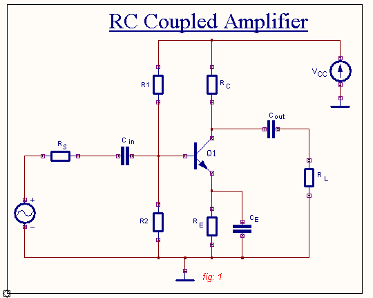
Design & Theory
DC Analysis
A transistor amplifier is designed to work in the active region. A single stage amplifier is designed using voltage divider bias. In a voltage divider
bias
the base voltage, VB is given by ![]()
 First we bias
the circuit in the active region with dc conditions.
![]() i.e.Current through R1, IR1 is a
large current of the order of 20 or 30 times that of IB.
i.e.Current through R1, IR1 is a
large current of the order of 20 or 30 times that of IB.
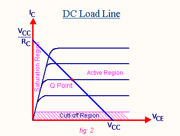
Current through R2, IR2 is given by ![]()
We select VCC as 10V.
![]()
Minimum Voltage Gain required = 100
![]()
Let ICQ = 2mA – ref. Manufacturer’s Datasheet
![]()
Applying Kirchoff’s Voltage Law for the output side of amplifier
![]()
![]()
![]()
![]()
![]()
![]()
![]()
Design of R1 & R2
For a fluctuation in IR1 and IR2
there will be small change in IB. For example as mentioned (ref. (5)),
if IR1=21IB and a 5% change in IR1
occurs there will be only ![]() change in
IB. Therefore the circuit will be stable against small changes in R1and R2 due to temperature or tolerance.
change in
IB. Therefore the circuit will be stable against small changes in R1and R2 due to temperature or tolerance.
Thus ![]()
And ![]()
![]()
![]()
=0.7+0.1VCC
![]()
From (8) ![]()
From (9) ![]()
![]()
![]()
![]()
AC Analysis
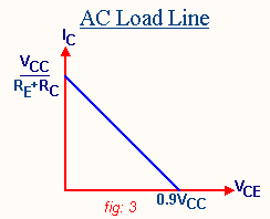
Modifications required from the dc circuit are
- Coupling capacitors (Cin, Cout)
- Bypass Capacitor CE.
The function of the coupling capacitor is to isolate the amplifier input circuit from the source. Since capacitor blocks dc it does not allow the dc components from the input circuit to get to the base of transistor and to change the Q point.
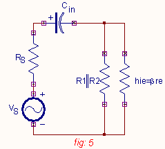
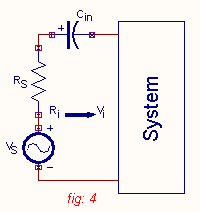
cut-off frequency; ![]() .
.
The LCF due to Cin; ![]()
At mid or high frequencies capacitor almost acts as a short circuit.
Then Vi is related to VS by; ![]()
![]()
![]()
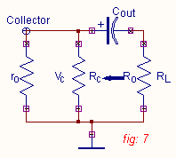
Effect of C/u>out
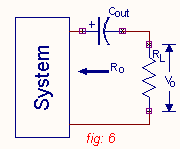
The effect of Cout on LCF is given by; ![]() where
where ![]() .
.
Effect of CE
CE is designed such that impedance of the capacitor
must be less than ![]() of RE
across which it is connected at LCF. The function of CE is to bypass the
emitter resistor during ac operation other wise during amplification with increase or
decrease in current, the drop across RE will increase or decrease and
hence VBE decreases or increases opposing the change in current. So the
function of RE is limited to
dc where the capacitor will be open and RE will stabilize
the circuit. In the case of ac the capacitor will take over current.
of RE
across which it is connected at LCF. The function of CE is to bypass the
emitter resistor during ac operation other wise during amplification with increase or
decrease in current, the drop across RE will increase or decrease and
hence VBE decreases or increases opposing the change in current. So the
function of RE is limited to
dc where the capacitor will be open and RE will stabilize
the circuit. In the case of ac the capacitor will take over current.
Form (15) ![]()
![]() hie =
1kW (datasheet)
hie =
1kW (datasheet)
![]()
Let fLin = 100Hz
![]()
![]()
![]()
![]()
![]()
![]()
![]()
![]()
![]()
![]()
where ![]()
For pn junction current I is related to voltage V
by equation ![]()
![]()
where h =1 for Ge and 2 for Si.
![]() where TC
is Room temperature in ° C
where TC
is Room temperature in ° C
TK = 25+273=298K
![]()
VT – Voltage equivalent of temperature
IS – Reverse saturation current
![]()
![]()
Now ![]()
![]()
![]()
Let fLE = 100 Hz
![]()
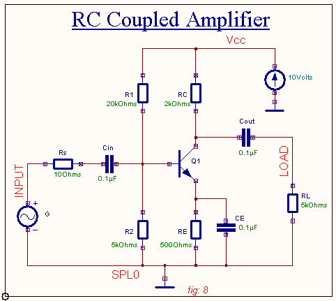
Note: - Some tolerances have been made in order to obtain standard values of components. All capacitors are designed to obtain a fair frequency response curve.
Procedure
Creating the Library Elements
To create a new part select EDWinXPMain -> Library -> Part Editor -> File -> New Part.
For e.g.: A transistor may be created in the following manner. Type in the information in the necessary fields (Prefix, Description,
Type, Manufacturer etc.). The symbol name may be given as NPN. It may be created manually or using Wizard. The symbol may be drawn using ‘Create Graphic Item’ function tool and its option tools. A filled bar is drawn using option tools rectangle and filled item. The filled triangle drawn using the option tools triangle and filled item represents the emitter and the direction of electron flow. Place the entries using ‘Create Entry’ option tool of ‘Create Graphic Item’ function tool. Then entries may be named as Emitter, Base and Collector using function tool ‘Edit Entry Attributes’. Now place the Component Name and Description appropriately.
In order to assign Simulation Names follow these steps. Select the ‘Properties’ function tool and its option tool ‘Symbol Properties’. Now select the desired simulation function from the list. Using ‘Edit Entry Attributes’ function tool click on each entry and assign proper Simulation Name to each pin. Save the Symbol/ Part either in user defined libraries and add them to the search sequence or in the Project Library itself.
Component placement
To place the components select Schematic Editor -> Components. The
components may be loaded in any of the following ways. Place these loaded components in the appropriate position using the
‘Relocate’ function tool and its option tool(s). Wires / Nets connection
To wire the components select Schematic Editor -> Wires & Buses. The ‘Route
Wire’ function tool and its appropriate option tool(s) may be used for this purpose. Enable option tool ‘Pin-to-pin routing’ for starting and
ending wiring from a component entry. Otherwise the routing may start very near to component entry which causes netlist problem. Prior to this
‘Instant Net Name’ and ‘Instant Wire Label’ may be enabled in‘Preferences’ menu, so that the net name can be given as required and
labels for the same can be placed without using any additional tool(s). Enable the option ‘Nodes’ in View menu, so that the
proper assignment of net to the component entries can be ensured Assign Values
The instance parameter (Component value) may be assigned either in Schematic
Editor or in Simulators. In Schematic editor this is performed using the function tool ‘Add/Change Component
text’ and its option tool ‘Add / Change Value’. It is mandatory to use
its option tool for this purpose and the simulators will ignore any values assigned
without using this option tool.
Preprocess
The purpose of preprocessing is to
establish the degree to which the circuit is ready for simulation. The results of preprocessing
are displayed in the "EDWinXP Info " window. This should be done
in both the simulators prior to performing any simulation. Simulation: Simulation is performed in both Mixed Mode
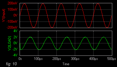
and EDSpice Simulator. In Mixed Mode simulator we are performing Transient Analysis, DC Sweep and AC Sweep Analysis. Mixed Mode Analysis Transient Analysis
In Transient Analysis, we perform the
simulation of the circuit and analyze the output voltage with respect to time. For this
maximum simulation time and the
time limit are set in the corresponding parameters window. Then simulation is performed with ‘Display
Waveform’
option enabled. The output of the amplifier is
viewed in the Waveform viewer. The user also has the provision to simulate with print
and plot
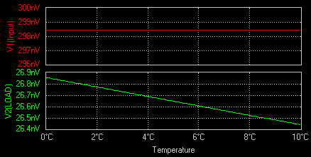
outputs. DC Sweep Analysis In this type of
analysis, usually temperature is the sweeping parameter. The user has the provision of sweeping parameters
of any two components at a
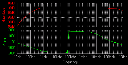
time. AC Sweep Analysis
AC Sweep
Analysis is performed for analyzing the frequency response of the circuit. It is required
to run AC Sweep Analysis after DC Sweep Analysis, so that the circuit operating
parameters would have been stabilized and set. The process is similar to
Transient analysis with difference
in the parameter setup. Simulation
Assign the parameters for each
and every component using the function tool ‘Set parameters/ models’ and its option tool
‘Set parameter’. Place
the test points appropriately so that the voltage
or current of that particular node or net has to be displayed. Now place
the waveform markers
at the node or net where the
waveform has to be observed. Preprocessing of the circuit must be carried out before
simulating it. Waveform Viewer Set all the necessary values in the waveform viewer as set in a
CRO.
Result The output waveform for various analyses is shown below. Mixed Mode Simulator Transient Analysis DC Sweep Analysis
