 View Video
Any trace segment may be assigned different widths at the start and at the end. When property
"Tapered" is set at the beginning of a segment,
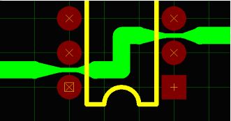
it will produce following results: If the width at the end of a segment is smaller then at the beginning, then the segment will taper
down gradually along its all length. In opposite case, such a segment will taper up from smaller to bigger width.
User may for example force selected or all segments in any trace to taper whenever there is a change of width from segment to segment.
This function creates smooth change of width in cases when thicker trace must be routed between pads.

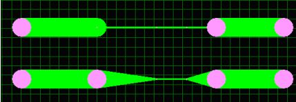
On request, all or selected trace segments may be automatically tapered to adjust to the size of the pad to which they are connected:

As seen on the picture above, ordering the thin trace segment to taper to a pad with bigger diameter produces similar
results as creating "tear drop" pads by adding copper elements (a method used in previous versions of EDWinXP).
The advantage of tapering is that there is no need to add any loose copper elements.
The old method for creating
"tear drop" pads has been retained for compatibility reasons .
Applies to
Layout Editor
1. Auto Taper trace segments  Purpose
Any trace segment may be assigned different widths at the start and at the end by setting Tapered property. You can taper selected or all segments in any trace whenever there is a change of width from segment to segment. This function creates smooth change of width in cases when thicker trace must be routed between pads. The advantage of tapering is that there is no need to add any loose copper elements.
Auto-taper trace functions allow executing following tasks:
- Taper trace segments in selected trace
- Taper trace segments in selected pad or point
- Taper trace segments for all PMD and SMD pads
- Removing taper for all pads on the board
- Removing selected taper
2. Taper trace segments in selected traces  Purpose
Allows to taper trace segments in selected traces
Operation
To taper trace segments of different width, Select

option tool or press Key F1 and then click on the desired trace to taper the trace segments. The bend points of the selected trace will get taper.
Note: Trace segments should be in different width.
3. Taper trace segments in selected pad or point Purpose
Allows to taper trace segments in selected pad or points
Operation
To taper trace segments in selected pad or point , Select

option tool or press Key F2 and then click on the desired pad or point to taper the trace segments. The selected node will get taper to the trace. A small conical shape inclined on node and the trace tapers the selected point or pad to the trace.
4. Remove Selected Taper  Purpose
Facilitates to remove selected taper
Operation
Select

or press Key F3, and click on the taper node which is to be removed.
5. Taper trace segments for all PMD pads  Purpose
Allows to taper trace segments for all PMD pads
Operation
Select

option tool or press Key F4, to taper trace segments of all PMD pads. All the PMD pads on the board will get taper to the corresponding trace segments.
6. Taper trace segments for all SMD pads  Purpose
Allows to taper trace segments for all SMD pads
Operation
Select

option tool or press Key F5, to taper trace segments of all SMD pads. All the SMD pads on the board will get taper to the corresponding trace segments.
7. Remove taper for all pads  Purpose
Facilitates to remove taper for all pads
Operation
Select

or Press Key F6, Connections window pops up. Click on Yes to remove taper for all pads.