Water Level Controller.
Aim:
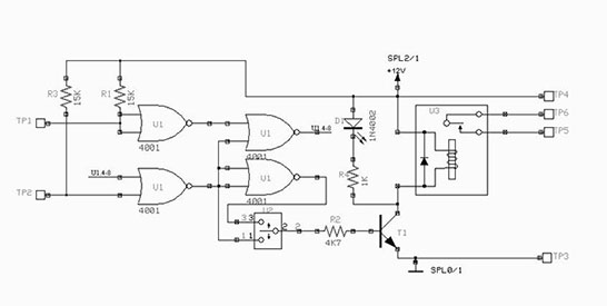
To design and simulate a Water Level Controller.
Schematic Diagram:
Components:
Theory:
Water level controller is an equipment used to control the water level in a field.This project controls the level of water in water tank automatically and is of better quality as compared to other circuits. This circuit sense the level of water at both at upper tank and lower tank because water goes from lower tank to upper tank.
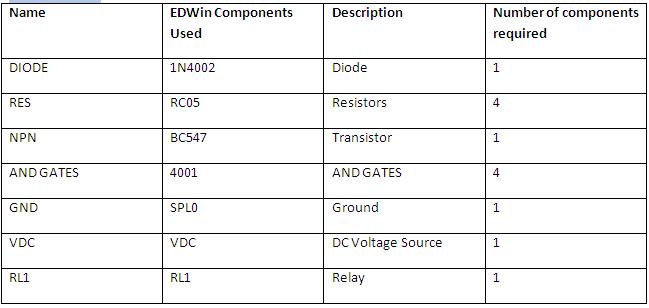
This circuit consists of four AND Gates with two inputs. Beside AND Gates a transistor is also used with the Gates.Relay is an electromagnetic device which is used to isolate two circuits electrically and connect them magnetically. They are very useful devices and allow one circuit to switch another one while they are completely separate.
PCB Layout:
PCB Layout is invoked from Project Explorer in the following ways.
Right click PCB Layout and select Edit PCB Layout from the list.
Or
Select Edit PCB Layout from the task list or from the task toolbar.
Define board outline
1. Select Tools --> Board Outline
2. Select Define Outline (function tool) --> Create Board (option tool). This tool enables free hand drawing, using which a board of desired shape can be drawn on the workspace.
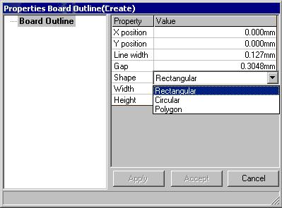
3. To select a pre-defined board format, select the option tool Textual Mode. The
Properties Board Outline (Create) dialog pops up.
4. Enter the desired values and click Accept button.
Relocating the components
The components placed on the schematic, which contain both symbol and package, are front annotated to the layout after packaging. These components are positioned at board datum (0,0) automatically and may be relocated either manually or automatically
Note: Only parts that contain both symbol and package will be automatically back annotated to the schematic.
1. Before we start loading Parts on to the page, turn ON
Grid by enabling grid from the dropdown, in Standard Toolbar. The value for grid may be selected from the drop down list as .1000".
2. Similarly, set Snap value to .0500” for better placement of the components.
3. Select Tools -->Components Relocate Component (function tool) to relocate the components.
4. Enable Ratsnest (F7 key) option tool of Relocate Component function tool to view ratsnest while relocating the components to ensure that components having a large number of interconnections are positioned close to each other. Pressing
shift key while relocating/ stretching an item allows the item to move/ stretch smoothly.
Routing the Components
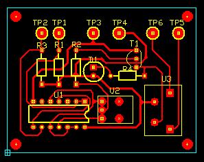
Connections between components may be established by using Traces and Copper Pour
areas.
1. Select Tools -->Connections --> Route (Function tool) to enable a set of Routing tools on right clicking the workspace.
2. Adjust zoom precision to view the pins properly.
3. Turn on Preference/ Guidelines (Next unconnected node) before routing because this option guides you to take the easiest path to route.
4. Select True Size and Pad frames from
View/ Layout, enabling you to select proper trace size. This also prevents you from creating errors such as traces crossing over pad, traces very close together etc.
5. First route power and ground signals (Net SPL0 and +5V). In Project Explorer, select Project / Project Design Rules and set the routing width to
0.030” for Pwr/Gnd lines and 0.013” for Signal lines.
6. To start routing traces, first select the power points
7. Select layer for routing from Layers in the main menu. 28 layers are available for routing. By default
COMP LAYER is selected. Click on pin to route on SOLD LAYER.
Tips: While routing, enable the tool  Snap Trace by 45 degree to change routing directions in steps of 45 deg only.
8. Move cursor with 45° angle through a short distance and click at the nearest point.
9. Terminate routing of the trace by pressing END or F4 key on your keyboard. Or click on the tool  End Connections.
3D View of the Board:
3D Board Viewer
3D Board Viewer gives idea on how the components are located, whether there is risk of friction between components due to their height and shape, the side on which components
are placed, etc.
Select Tools --> 3D Board Viewer to view the 3D board
3D View Control box appears, in this we can select options to view the board in any direction.
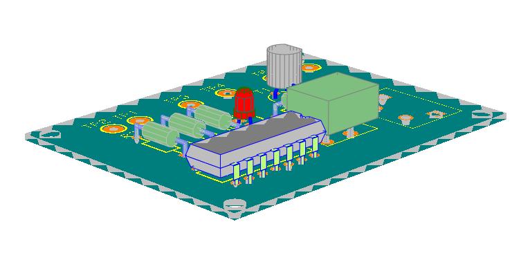
3D Board View
The actual size (1:1) of the board is given below
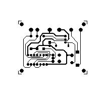
Solder Layer
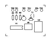
Component Print Layer