Standards for Drawing Schematic Symbols in EDWinXP
Library
ANSI Method
GRID
All Schematic Symbols should be placed on a grid of 100 mil.
GRID
All Schematic Symbols should be placed on a grid of 100 mil.
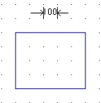
SNAP
Snap settings that should definitely be followed are specifically mentioned wherever required.
SYMBOL OUTLINE
For rectangular symbols, Width-Height ratio of the symbol should preferably be 1:3. In situations where this is practically not feasible, rectangles / squares of suitable sizes may be used. The rectangles / squares should be a single graphic item and must NOT be made by lines or multiple graphic items.
PIN LENGTH
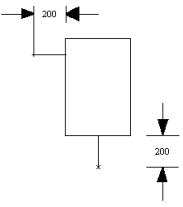
Pin length should be 200 mil under all circumstances. (Unless other wise specified). This is exempted for OPAMP like symbols. The pin length should be suitably selected in the se cases.
PIN TO PIN GAP
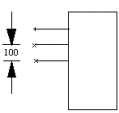
Space between consecutive pins should be 100 mil. (Unless other wise specified).
Space between consecutive pins should be 100 mil. (Unless other wise specified).
ENTRY PLACING / NUMBERING
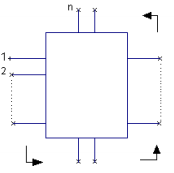
The first entry should be placed on the top left corner pin. The remaining entries should be placed in the anti-clockwise direction, in continuous fashion, until the last pin.
The first entry should be placed on the top left corner pin. The remaining entries should be placed in the anti-clockwise direction, in continuous fashion, until the last pin.

PA SHIFT
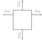
At a snap of 20 mil, PA shift should be placed 20 mil to the right/left and 20 mil to the top/bottom of the entry. PA should be readable in the standard projection views.
At a snap of 20 mil, PA shift should be placed 20 mil to the right/left and 20 mil to the top/bottom of the entry. PA should be readable in the standard projection views.
LINE SIZE
The line size (thickness) of all graphic items should be 8 mil. This is exempted for some special cases like Cathode of a diode.
TEXT SIZE & PITCH
The size of all texts including COMPNAME and COMPDESC should preferably be 60 mil. The pitch of text should be 24 mil. For very large symbols, text sizes of COMPNAME and COMPDESC should be suitably increased. The aim is to show the names if the size is reduced below 1:1.In the case of large symbols, the COMPNAME and COMPDESC should suitably increase in the multiples of 60 mils. The line thickness of the same should NOT be more than 8 mil in any case.
TEXT POSITION
Texts should be placed within the symbol and 20 mil away (left / right / top / bottom) from the boundary of the symbol. Text placing in the symbol may be avoided in the case of standard symbols. The position of text placing is exempted in the case of special symbols like OPAMP.
POSITIONING OF COMPNAME & COMPDESC
These should be placed within the symbol as far as possible. Whe rever this is not possible, they should be placed as close to the symbol as possible. This is for avoiding the confusion between two adjacent symbols.
TEXT NAME (PIN NAME)
Text names should be small, meaningful and should express the function of the pin. In case of multiple pins with same function, they should be numbered consecutively with its pin function name. However, multiple GNDs and VCCs should NOT be numbered consecutively because they form a single net.
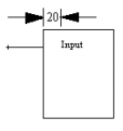
The entry names of the above should be numbered consecutively with their pin
function names. Eg: For multiple INPUT, the text names as INPUT1, INPUT2 etc.
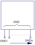
and entry names as INPUT1, INPUT2. For multiple GND, the text names as GND, GND
etc. and entry names as GND1, GND2. The positions of consecutive pin text names
should start from Left to Right and Top to Bottom. In the case of multiple GND
pins the entry names should start from GND1 to GNDn and the pin text should be
simply only one GND and not as GND1 to GNDn provided all GND pins at the same
voltage level.
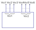
Exemptions are made only if full information of the pins is not available. This
GND (pin text name) should be with a bracket which will represent all GND pins
of same voltage level For multiple supply pins (Vcc, Vdd etc) the same rule as
above should be followed If supply pins are at different voltage levels, those
at the same voltage level should group together.
ENTRY ATTRIBUTE
Entry attribute should be the name of the pin. For negated signal conditions, a TILDE (~) should be used before the name of the pin.
Entry attribute should be the name of the pin. For negated signal conditions, a TILDE (~) should be used before the name of the pin.
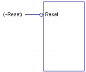
In the case of very long pin names, the entry name may be truncated with 2/3 of
the pin name. In the case of space between characters in pin names, the same
should be replaced

by a hyphen (-) in entry names.
 Note: Entry attribute of ANSI / IEC of same symbol should be unique.
POSITIONING OF PINS
All inputs should be on the left side and outputs on the right side of the symbol. (Unless other wise specified) For very big symbols, the inputs may be 2/3 of all pins.
 Note: Entry attribute of ANSI / IEC of same symbol should be unique.
POSITIONING OF PINS
All inputs should be on the left side and outputs on the right side of the symbol. (Unless other wise specified) For very big symbols, the inputs may be 2/3 of all pins.
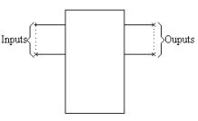
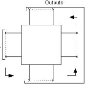
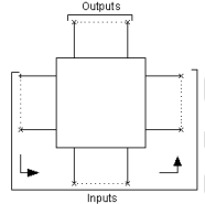
In this situation the inputs may be placed in three sides of the symbol starting
from top left corner and ending at top right corner. If the output pins are 2/3
of all pins we can keep inputs and control pins in the left side and outputs
starting from bottom left and ending at top left of the symbol. Inputs contain
input pins, control pins, GND pins while output contains output and supply pins.
Exemptions may be made depending on the complexity of the symbol. This is
subjected to approval from QA Dept.
LOCATION OF SUPPLY PINS
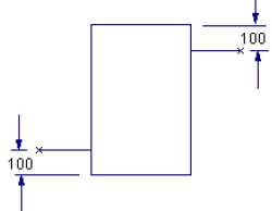
(a) For rectangles using only two sides +ve power supply (+Vcc) pins should be on top right corner, -ve power supply (-Vcc) should be on the bottom right and the GND should be on the bottom left si de of the rectangle. The distance between the last GND and bottom corner of rectangle should NOT be more than 100 mil in any case.
(a) For rectangles using only two sides +ve power supply (+Vcc) pins should be on top right corner, -ve power supply (-Vcc) should be on the bottom right and the GND should be on the bottom left si de of the rectangle. The distance between the last GND and bottom corner of rectangle should NOT be more than 100 mil in any case.
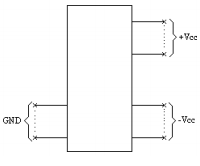
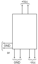
(b) For rectangles using all sides +ve power supply (+Vcc) pins should be on top
side and -ve power supply (-Vcc) should be on the bottom side of the rectangle.
GND should be on the bottom left side of the rectangle. The distance between
last GND and bottom corner of rectangle should not be more than 100 mil in any
case. The position of GND pins may change to bottom side according to number of
input side pins.
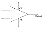
(c) For symbols using other graphic items In all other cases +ve power supply
pins should be on top side and -ve power supply should be on the bottom of the
symbol. (Unless other wise specified)
GLOBAL NET
Global net will be assigned when the no. of Analog Supply / GND pins exceed 4 pins. One entry should be drawn in the schematic symbol which represents all other pins that come under that global net. Its entry name should be same as the name of Global net. The method of naming Global nets is as VDD3V for 3V VDD Supply, VDD (-3V) for –3V VDD and VDD (-5to3V) for the voltage range of –5 to 3V. Global nets are assigned while the creating the. (In exactly same way as assigning digital supplies (SPLs)). All net names should be as per the manufacturer specification. (Eg. VDD, Vdd, VSS, Vss etc...)
LOCATION OF REFERENCE VOLTAGES (V+, V-)
Positive reference voltage (V+) should be on the top left. Similarly -ve reference voltage (V-) should be put on the bottom left corner, before the GND pin of the symbol outline.
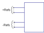
Eg: +5V, +10V may be considered as Reference Voltages. RefGND also may be placed
before the ordinary GND pins.
GROUPING OF PINS
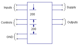
Similar (related signal) pins should be grouped together. Eg: Input pins, Data pins, Address pins, Control pins, Output pins etc. 200 mil gaps should be left between two adjacent groups.
Pins within a single group should be named consecutively from left to right / top to bottom. Eg: I/O 1, I/O 2, I/O 3 etc.
Supply and Ground pins also should be grouped.
REPETITION OF SYMBOLS
Within the same Device Family / Library the same symbol should not be copied into different names However, they may be copied into different Device Families. Different symbols should be used for different manufacturer’s devices: even for those that are functionally similar.
 Note: Will be revised later to take into consideration for simulation purposes.
Eg: Same symbol can be used for 7400, 54F00, 74HC00 even if the manufacturer is
different. ADC1450 is manufactured by Linear Technology Corporation and
Burr-Brown. Different symbol should be used in these cases and naming of symbol
should be different.
DISTANCE BETWEEN PIN AND BOUNDARY
Distance between the outermost pin and the nearest corner should be 100 mil. (Exceptions exist for large symbols)
Within the same Device Family / Library the same symbol should not be copied into different names However, they may be copied into different Device Families. Different symbols should be used for different manufacturer’s devices: even for those that are functionally similar.
 Note: Will be revised later to take into consideration for simulation purposes.
Eg: Same symbol can be used for 7400, 54F00, 74HC00 even if the manufacturer is
different. ADC1450 is manufactured by Linear Technology Corporation and
Burr-Brown. Different symbol should be used in these cases and naming of symbol
should be different.
DISTANCE BETWEEN PIN AND BOUNDARY
Distance between the outermost pin and the nearest corner should be 100 mil. (Exceptions exist for large symbols)
NAMING CONVENTIONS FOR SCHEMATIC SYMBOLS
Names should be given in such a way that it will express the function of the of the Device. However it is not necessary to give full Device name in the name of Schematic Symbol. Schematic Symbol names should preferably include the function and a part of Device name in a meaningful fashion.
If the same Schematic Symbol is used by more than one Device, a common name, which is representative, may be used. Common examples are given below.
In EDWinXP Library BUF 470 is used by 74470 and 74471. 74 is common for Digital Devices and remaining is 470 and 471 then better use the name BUF 74x or something like this. Names such as BUF 1 , BUF[1] , BUF(1) etc. should not be used.
REPRESENTATION OF SUBSCRIPTS IN NAMES
All subscripts should be lower case letters.(Subscripts are used only as specified by the manufacturer.) Eg: Vcc , Vin , Vout etc.
REPRESENTATION OF NEGATED SIGNALS USING BUBBLES AND BAR
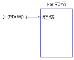
Use bubbles where ever possible. Avoid bubbles when two signals carrying a pin with different logic signals are used. Eg: RD/W
In this case the pin-text name should be as RD/W and draw a bar for W with a graphic item (line).
The entry name for the same will be (RD/~W). Pin text name should not be represented with a Tilde (~) in the case of negated symbol.
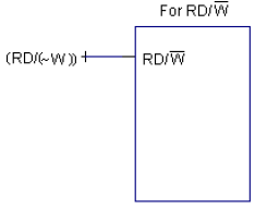
Eg: RD/W In this case the pin-text name should be as RD/W and draw a bar for W
with a graphic item (line).
The entry name for the same will be (~ (RD/W)).
The entry name for the same will be (~ (RD/W)).
IEC
Method SYMBOL
When creating an IEC symbol, all IEC rules should be strictly followed. i.e., the symbol should be an exact copy of the one in the data book. All exceptions are specifically mentioned, wherever applicable.
GRID
All Schematic Symbols should be placed on a grid of 100 mil. SNAP Snap settings that should definitely be followed are specifically mentioned wherever required.
PIN NAMES
Since pin names are given as entry attributes no specific pin names are to be given when creating IEC symbols.
PIN LENGTH
Pin length should be 200 mil under all circumstances. (Unless other wise specified)
ENTRY PLACING / NUMBERING
The first entry should be placed on the top left corner pin. The remaining entries should be placed in the anti-clock wise direction, in continuous fashion, until the last pin.
When copying an existing symbol to be used as a template for creating new symbols, entries should be renumbered according to the above fashion.
In all cases regardless of symbol size & shape, the 1st entry should be on the top left corner.
PA SHIFT
At a snap of 20 mil, PA shift should be placed 20 mil to the right/left and 20 mil to the top/bottom of the entry. PA should be readable in the standard projection views.
LINE SIZE
The line size (thickness) of all graphic items should be 8 mil.
TEXT SIZE & PITCH
The size of all texts including COMPNAME and COMPDESC should preferably be 60 mil.
The pitch of text should be 24 mil.
For very large symbols, text sizes of COMPNAME and COMPDESC should be suitably increased. The aim is to show the names if the size is reduced below 1:1.
IIn the case of large symbols, the COMPNAME and COMPDESC should suitably increased in the multiples of 60 mils. The line thickness of the same should NOT be more than 8 mil in any case.
TEXT POSITION
Texts should be placed within the symbol and 20 mil away (left / right / top / bottom) from the boundary of the symbol.
POSITIONING OF COMPNAME & COMPDESC
These should be placed within the symbol as far as possible. Wherever this is not possible, they should be placed as closed to the symbol as possible. This is for avoiding the confusion between two adjacent symbols.
NAMING CONVENTIONS FOR SCHEMATIC SYMBOLS
Names should be given in such a way that it will express the function of the of the Device. However it is not necessary to give full Device name in the name of Schematic Symbol.
Schematic Symbol names should preferably include the function and a part of Device name in a meaningful fashion. If the same Schematic Symbol is used by more than one Device, a common name, which is representative, may be used. Common examples are given below.
In EDWinXP Library BUF 470 is used by 74470 and 74471. 74 is common for Digital Devices and remaining is 470 and 471 then better use the name BUF 74x or something like this.
NNames such as BUF 1, BUF [1] , BUF(1) etc. should not be used.
REPRESENTATION OF SUBSCRIPTS IN NAMES
All subscripts should be lower case letters. (Subscripts are used only as specified by the manufacturer.) Eg: Vcc, Vin, Vout etc.
ENTRY ATTRIBUTE
Entry attribute should be the Pin Name, which is shown at the Pin’s outer side.
 Note: Entry attribute of ANSI/IEC of same symbol should be unique.
Method SYMBOL
When creating an IEC symbol, all IEC rules should be strictly followed. i.e., the symbol should be an exact copy of the one in the data book. All exceptions are specifically mentioned, wherever applicable.
GRID
All Schematic Symbols should be placed on a grid of 100 mil. SNAP Snap settings that should definitely be followed are specifically mentioned wherever required.
PIN NAMES
Since pin names are given as entry attributes no specific pin names are to be given when creating IEC symbols.
PIN LENGTH
Pin length should be 200 mil under all circumstances. (Unless other wise specified)
ENTRY PLACING / NUMBERING
The first entry should be placed on the top left corner pin. The remaining entries should be placed in the anti-clock wise direction, in continuous fashion, until the last pin.
When copying an existing symbol to be used as a template for creating new symbols, entries should be renumbered according to the above fashion.
In all cases regardless of symbol size & shape, the 1st entry should be on the top left corner.
PA SHIFT
At a snap of 20 mil, PA shift should be placed 20 mil to the right/left and 20 mil to the top/bottom of the entry. PA should be readable in the standard projection views.
LINE SIZE
The line size (thickness) of all graphic items should be 8 mil.
TEXT SIZE & PITCH
The size of all texts including COMPNAME and COMPDESC should preferably be 60 mil.
The pitch of text should be 24 mil.
For very large symbols, text sizes of COMPNAME and COMPDESC should be suitably increased. The aim is to show the names if the size is reduced below 1:1.
IIn the case of large symbols, the COMPNAME and COMPDESC should suitably increased in the multiples of 60 mils. The line thickness of the same should NOT be more than 8 mil in any case.
TEXT POSITION
Texts should be placed within the symbol and 20 mil away (left / right / top / bottom) from the boundary of the symbol.
POSITIONING OF COMPNAME & COMPDESC
These should be placed within the symbol as far as possible. Wherever this is not possible, they should be placed as closed to the symbol as possible. This is for avoiding the confusion between two adjacent symbols.
NAMING CONVENTIONS FOR SCHEMATIC SYMBOLS
Names should be given in such a way that it will express the function of the of the Device. However it is not necessary to give full Device name in the name of Schematic Symbol.
Schematic Symbol names should preferably include the function and a part of Device name in a meaningful fashion. If the same Schematic Symbol is used by more than one Device, a common name, which is representative, may be used. Common examples are given below.
In EDWinXP Library BUF 470 is used by 74470 and 74471. 74 is common for Digital Devices and remaining is 470 and 471 then better use the name BUF 74x or something like this.
NNames such as BUF 1, BUF [1] , BUF(1) etc. should not be used.
REPRESENTATION OF SUBSCRIPTS IN NAMES
All subscripts should be lower case letters. (Subscripts are used only as specified by the manufacturer.) Eg: Vcc, Vin, Vout etc.
ENTRY ATTRIBUTE
Entry attribute should be the Pin Name, which is shown at the Pin’s outer side.
 Note: Entry attribute of ANSI/IEC of same symbol should be unique.