CONTENTS
EDWinNET 1.0 Standard version comes with all Standard features of EDWinXP. This is the conversion and movement of EDWinXP to a new platform, .NET. This has several features in Schematic Editor,PCB layout and Fabrication Manager with new appearance and which can be used easily than the EDWinXP.
The following details of EDWinNET will helps you to use this software more easily.
Schematic Editor
Invoke Schematic Editor from Project Explorer in the following ways
Right click Page [Main Page] and Select Edit Page from the list.
Or
Select Edit Page from the task list or from the task toolbar.
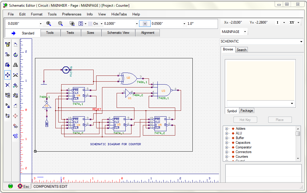
1. Turn ON Grid 
2. The value for grid may be selected from the drop down list as .1000”.
3. Set Snap value to .0500” for better placement of the components.
 Loading the Components
Select Tools | Components toolbar and right click on the workspace to popup a set of Component editing tools. By default, relocate tool is enabled.
 Loading Components using Component Browser
1. The component browser is launched from View | Schematic | Browser.
2. The required components can be obtained either by using the Browse option in the window or by Search for the element in the quick menu
3. Using the Place button in the bin we can place the components in the workspace.
Note: Hotkeys can also be assigned to element names by which quick launch of components is possible.
4. Voltage source, Ground and signal generators can be obtained from the Component Browser. These are external sources (which will not be housed on the PCB) and hence connections to them can be shown with the help of connectors. Select connectors from the component browser, then select List Connector and select the required header from the list appearing.
5. Load the connector and using Repeat Component function tool, create the required number of instances. Similarly load SPL0 (Hotkey G).
6. To relocate the component, right click and select tool Relocate. Position the part where required and click the mouse to place component
 Packaging the Components
If the PCB of the circuit has to be designed, then the components need to be packaged. Packaging is nothing but information that the system requires identifying the Package associated to Part placed on the Schematic. Only packaged components are automatically front annotated to layout.
 Auto Packaging
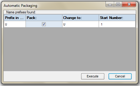
Select Tools | Component | Pack/Unpack Component | Auto packaging from the option tool. An Automatic Packaging window appears Click Execute button.
 Routing the wire connections
1. Connections between components are established using wires and buses.
2. Select Tools | Connections to enable a set of tools required for routing.
Tip: Adjust zoom precision to view the terminals being wired. Turn ON grid and snap to help in positioning the wires.
3. Before creating the connections, enable Preferences/Instant net name and Preferences/Instant wire label.
4. Right click on the work space and select Connections.
5. Enable Pin to Pin option tool whenever an entry or pin is clicked for making a connection. This ensures that the connection is made to the pin.
6. An input box appears prompting the user to enter the name of the net, enter the name most suited for the net.
 Viewing the output
1. Select Tools | Instruments Set wave form Contents (function tool) |Voltage Waveform (option tool).
2. Click on the nets where the voltage waveforms to be displayed.
 Entering Page Notes and Design Notes
1. Page notes appear only on the current page (e.g. Page No.) of the project whereas Design notes appear on all the pages (e.g. Project name) of the selected circuit.
2. Select Tools | Page Notes toolbar to enable a set of tools for creating page notes. Right click and enable
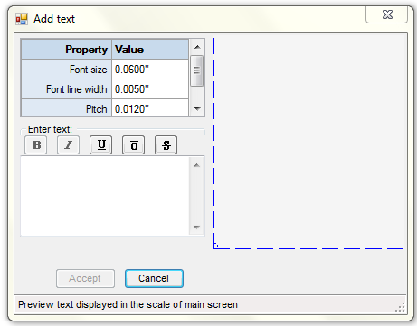
3. Create PN Graphic Item tool | Create Text to open a window Edit & Add Text block. Enter the required notes and accept it.
The text gets tagged to the cursor. Now place the text at desired position. To edit this text, Press Ctrl key and click on the text to select it. Perform the various operations using bullets.
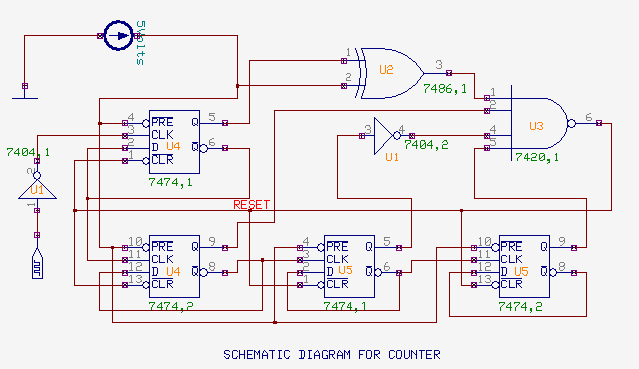
Schematic Circuit designed is given below.
 Saving the Project
In order to prevent loss of work, save the project periodically using the following steps.
1. On the File menu of Project Explorer, Click Save Project or Press Ctrl + S.
2. The first time Save Project is selected, a dialog pops up prompting to enter the name for the project.
3. Type in the name of project as Counter.EPB.
 Printing the Schematic Diagram
To print the Schematic diagram,
1. Select File | Print page from the main menu of Schematic Editor.
2. A window pops up with the preview of circuit diagram.
3. Click on ‘Fit graphic to one page with margin’ icon. Click on Print Page icon to print the page.
Simulation
 Mixed Mode Simulation
Steps for Mixed Mode Simulation
Preprocess the circuit
The simulator analyzes the schematic first and checks for the simulation function. It generates the data along with the statistics of the circuit. Data includes the number of digital and analog nets, list of symbols, which may be simulated along with their simulation functions, number of digital inputs and outputs, number of A/D input/ outputs. This is presented as a dialog box. Observe that the analog primitives are assigned negative simulation function.
Click the OK button to close this dialog box. The simulator is now ready for making further analysis on the circuit.
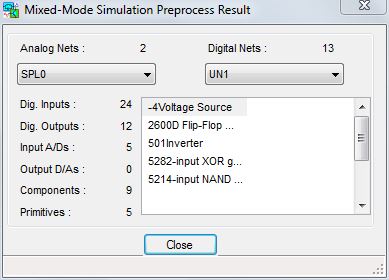
Note: Any change in the circuit element values or topology gets implemented only if the preprocess is invoked. Preprocess menu is invoked from Simulation menu. Preprocessing the circuit resets the values set.
 Assign Component Parameter Values
1. Select Component Properties (function tool)-->Change Simulation Parameters (option tool).Click on the component
2. Component Parameter Setup window opens.
3. Change the parameter values.
4. Click Accept.
 Analysis
For setting up simulation time and Start analysis types,
1. Select Simulation -->Analysis.
2. Set the parameters by selecting General settings from the tree view on the left side of the window.
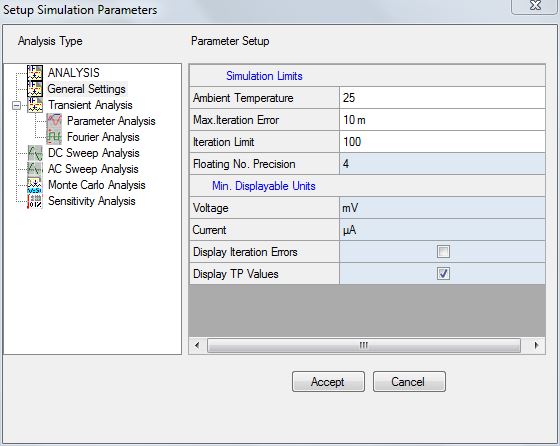
3. Set the values as
Simulation Limits:
Ambient Temperature -->25
Max. Iteration Error -->100m
Iteration Limit--> 100
Floating No. Precision--> 4
Min. Displayable Unit:
Voltage mV
Current μA
4. Click Accept button to accept the changes and to automatically switch to Analysis option
 Bias Point Calculation
Bias Point Calculation is used to determine the DC behaviour of the circuit.
1. Inorder to view the DC values, fix the test points at the base, collector and emitter of the transistor as shown below. To place the test points, select Tools -->Instruments


2. Select Simulation --> Analysis.
3. A window Setup Simulation Parameters opens with the option Analysis being highlighted on the left side of the window by default.
4. Check Bias Point Calculation check box.

Click Start button, and observe that the node voltages are displayed at the locations where test points were placed. Similarly current values can also be viewed by placing the test points at the required nets.
 Transient analysis
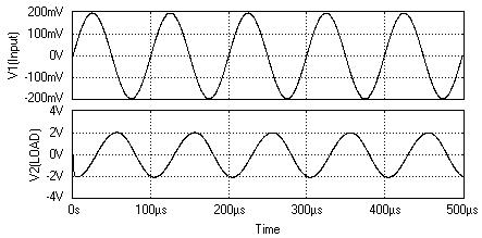
Transient analysis is used to view the input and output with respect to time. Inorder to view the performance of the circuit in time frame run transient analysis.
1. Select Simulation --> Analysis.
2. Select Transient analysis from tree view.
3. Enter following values:
Analog simulation step time: 2μ
Simulation time limit: 1m
4. Check Display waveform check box.
5. Click on Accept to switch into the Analysis option
6. Click Start to begin the analysis.
 Parameter Analysis
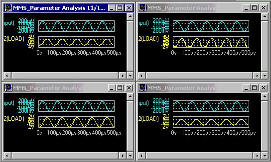
Parameter analysis helps to study the effect of variation of component parameters on the circuit. This analysis calculates the change in the output of a given circuit when a selected parameter of a particular circuit element is varied over a range of values.
1. Select Simulation --> Analysis.
2. Select Parameter Analysis from the tree view.
3. Select Sweep Variable as Component Parameter type.
4. Move the cursor over the resistor and click on it. Selected component name and parameter name appears in the dialog box.
5. Set the values for the following parameter as
Start Value -->1K Ohm
End Value--> 3K Ohm
Steps--> 750 Ohm
6. Click Accept to switch into Analysis option.
7. Check Parameter analysis check box.
8. Now click Start button for analysis to take place. The result may be viewed in the Waveform viewer.
 Fourier Analysis
Fourier analysis helps to calculate the total harmonic distortion of analog waveforms generated during transient analysis.
1. Select Simulation--> Analysis.
2. Select Fourier analysis from the tree view.
3. Set the parameters in the box as
Fundamental Frequency -->10K
No of harmonics (nfreq) -->10
Deg. of Polynomial (polydegree)--> 2
4. After setting the parameter click Accept button to accept the parameters.
5. Check Fourier Analysis and click Start button. Fourier analysis results are displayed in a text format.
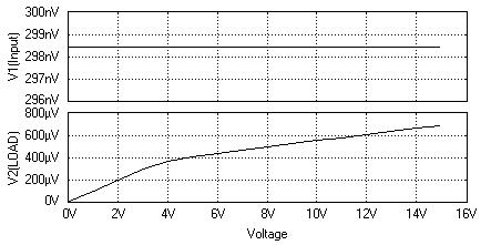
 DC Sweep Analysis
DC Sweep analysis helps to observe the circuit operating parameters by varying the value of a component. One or more sources (current and voltage) may be stepped over a range. Results of the analysis at each source value may then be viewed in the waveform generator.
1. Select Simulation --> Analysis.
2. Select DC Sweep Analysis from the tree view.
3. Move the cursor over DC supply and click on it. Selected component name and parameter name appears in the dialog box.
4. Set the sweep limits as
Start value--> 0V
End value -->15V
Steps--> 1V
5. Check Display Waveform check box to display the waveform.
6. Select Accept to switch into Analysis Option.
7. Check DC Sweep Analysis check box.
8. Click Start
 AC Sweep Analysis
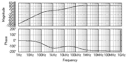
AC sweep analysis is used to calculate the small signal frequency response of the circuit assuming its current biasing.
1. Select Instruments -->  Set Reference Points (function tool) -->
 AC IN+ and click on the input net.
2. Select Instruments -->  Set Reference Points (function tool)
-->
  AC IN- option tool and click on the input net.
3. Note: This tool specifies the input given to the input side to be a voltage source or a current source for running the AC Sweep Analysis.
4. Select Instruments--> Set Reference Points  -->AC OUT+
  and click on the load net.
5. Select Instruments-->Set Reference Points  --> AC OUT-
  and click on the load net.
6. Note: This tool specifies the output variable taken from the output side to be either the open voltage or the short current.
7. Select Simulation--> Analysis
8. Select AC Sweep Analysis from the tree view.
9. Set the values for the following parameters as
Start frequency -->100 Hz
End frequency--> 1GHz
Points / decade--> 100
Phase range--> [-180, +180]
IN source--> voltage
OUT source--> Open voltage
10. Click Accept button to switch into Analysis option.
11. Check AC Sweep Analysis check box.
 Monte Carlo Analysis
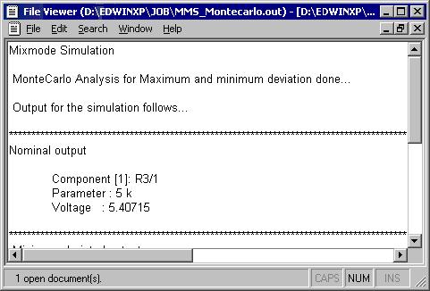
The Monte Carlo analysis is used for simulations with a given error on different components. This test is very useful for visualizing how the circuit will run with imperfect components as are used in reality.
1. Select Simulation --> Analysis.
2. Select AC Sweep Analysis from the tree view.
3. Select Instruments--> Set Reference Points --> Monte Carlo voltage
and click on any of the nets.
4. Select Monte Carlo Analysis from the tree view.
5. Select the component at which the analysis has to be done, by clicking on it.
6. Enter the parameters and click Accept to accept the parameters.
7. Click Start.
The result is displayed in a text file.
 Sensitivity Analysis
Sensitivity Analysis is used to calculate the component that is most sensitive to an output reference point.
1. Select Simulation --> Analysis.
2. Select Sensitivity Analysis from the tree view.
3. Inorder to determine the sensitivity of a component with reference to a net select
Instruments -->
Set Reference Points -->Sensitivity voltage
4. Click on any of the nets and place the reference points.
5. Select Sensitivity Analysis from the tree view.
6. Specify a value of tolerance for which the analysis is to be carried out. This is the common tolerance value for all parameters of all components.
7. Click Accept button to switched into Analysis option.
8. Check Sensitivity Analysis check box.
9. Click Start button, result is displayed in a text file.
PCB LAYOUT
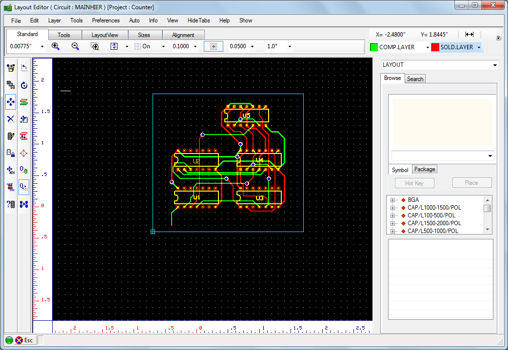
PCB Layout is invoked from Project Explorer in the following ways.
Right click PCB Layout and select Edit PCB Layout 
Or
Select Edit PCB Layout from the task list or from the task toolbar
 Define board outline
1. Select Tools | Board Outline
2. Select Define Outline (function tool) | Create Board (option tool). This tool enables free hand drawing, using which a board of desired shape can be drawn on the workspace.
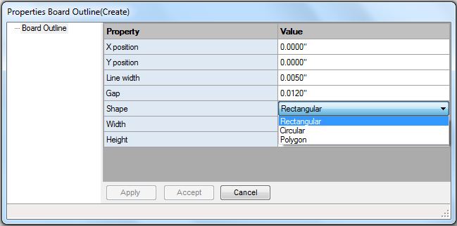
3. To select a pre-defined board format, select the option tool Textual Mode. The Properties Board Outline (Create) dialog pops up.
4. Enter the desired values and click Accept button.
 Relocating the components
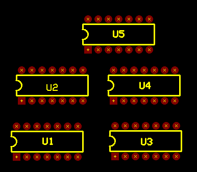
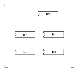
The components placed on the schematic, which contain both symbol and package, are front annotated to the layout after packaging. These components are positioned at board datum (0,0) automatically and may be relocated either manually or automatically
Note: Only parts that contain both symbol and package will be automatically back annotated to the schematic.
1. Before we start loading Parts on to the page, turn ON Grid by enabling grid from the dropdown, in Standard Toolbar. The value for grid may be selected from the drop down list as .1000”.
2. Similarly, set Snap value to .0500” for better placement of the components.
3. Select Tools | Components | Relocate Component (function tool) to relocate the components.
4. Enable Ratsnest (F7 key) option tool of Relocate Component function tool to view ratsnest while relocating the components to ensure that components having a large number of interconnections are positioned close to each other. Pressing shift key while relocating/ stretching an item allows the item to move/ stretch smoothly.
 Routing the Components
Connections between components may be established by using Traces and Copper Pour areas.
1. Select Tools | Connections | Route (Function tool) to enable a set of Routing tools on right clicking the workspace.
2. Adjust zoom precision to view the pins properly.
3. Turn on Preference/ Guidelines (Next unconnected node) before routing because this option guides you to take the easiest path to route.
4. Select True Size and Pad frames from View/ Layout, enabling you to select proper trace size. This also prevents you from creating errors such as traces crossing over pad, traces very close together etc.
5. First route power and ground signals (Net SPL0 and +5V). In Project Explorer, select Project / Project Design Rules and set the routing width to 0.030” for Pwr/Gnd lines and 0.013” for Signal lines.
6. To start routing traces, first select the power points
7. Select layer for routing from Layers in the main menu. 28 layers are available for routing. By default COMP LAYER is selected. Click on pin to route on SOLD LAYER.
Tips: While routing, enable the tool 
8. Move cursor with 45° angle through a short distance and click at the nearest point
9. Terminate routing of the trace by pressing END or F4 key on your keyboard. Or click on the tool
 Auto Routers
The three Auto routers available are:
1. Autorouter-Arizona
2. Autorouter-Specctra
3. Autorouter-Maxroute
 Arizona Autorouter
Arizona auto router is an integrated module of the EDWinXP. It uses its own temporary project and simplified graphics. The Arizona auto router allows routing the traces of a PCB Layout automatically
 Auto routing using Arizona Auto router
1. Select Auto | Auto Router | Arizona.
2. Select File | Load board to route from project.
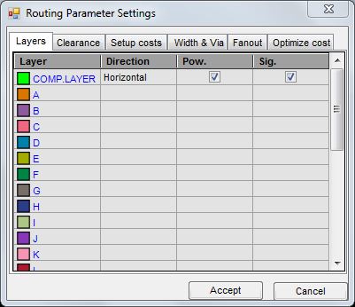
3. Select Parameters Setup (function tool) | Routing Parameter Settings (option tool).
4. Check Solder Layer in the Routing Parameters Settings window
5. Select Auto routing Routines (function tool) | Start Auto Router.
6. Select Auto routing Routines | Miter.
7. Close Arizona Auto router window, Click Update project and Exit to save the project.
 Testing the Board
While designing a PCB, it is quite obvious that a number of errors may occur. These errors may be in the form of overlapping pads, unconnected Nodes, traces crossing another trace, etc. Such errors must be taken care of before printing the PCB. To find out such errors, certain checks on the board are done. Connectivity and DRC check are the two checks.
 Connectivity Test
Connectivity test may be used to check whether there is any electrical discontinuity (unconnected nodes or deleted trace segments) in a single net. By setting certain parameters, the test can be performed either on individual nets or all the selected nets.
1. Select Tools | Connections | Connection Property | Test Connectivity
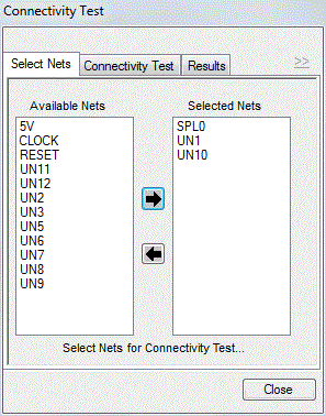
2. Click on the board or on a net. The Connectivity Test dialog pops up.
3. Select the required nets using the move keys and click the connectivity test tab.
4. Select Connectivity test tab, set anyone of the three options:
Stop at first fail: Test stops at the first occurrence of error.
Test all selected Nets: Checks whether all Nodes of the selected Nets are connected.
Test single Net: Checks connectivity of the Nodes of the selected Net.
5. Click the Test button to display the results.
6. Perform this test until “Tested Nets – Fully Connected” message is displayed in this window.
 Design Rule Check (DRC)
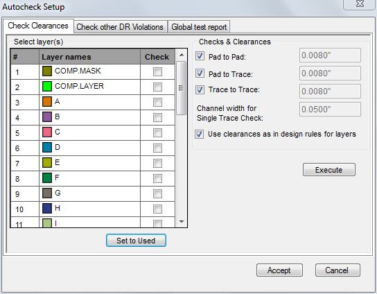
This utility is used to create an error free board to enhance the efficiency of your board. It automatically smoothes, miters, and checks for both aesthetic and manufacturing problems that might have been created in the process of manual or automatic routing. This test helps us to check the clearance between pad to pad, pad to trace and trace to trace.
Select Autocheck from Auto Menu. The Clearance Check dialog pops up.
Select the layers and enter the clearance value in the window.
To select all the layers used in the project click the Set To Used button.
Click Execute
Board Analyzers
EDWinXP provides two board analyzers.
Thermal Analyzer
Electromagnetic Analyzer
 Thermal Analyzer
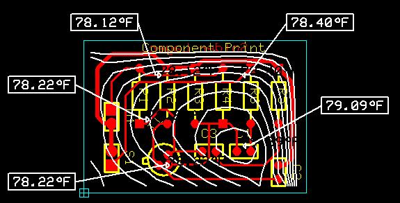
The Thermal Analyzer is intended to be used for analyzing and identifying potential thermal problems on a Printed Circuit Board. It evaluates the Temperature Distribution on a finished PCB, at steady state conditions.. The result of the analysis may be displayed using isotherms or color mapping scheme.
 Steps for Thermal Analysis
1. Right click on the PCB Layout in the Project Explorer. Select Board Analyzer in the list.
2. Select the Thermal Analyzer tab.
3. From Analysis, choose Settings to open the settings window and click the Display Options tab. Click on Set to default button .
4. From the Analysis menu select Settings click and select the tool
Board Parameters Click on Set to default button
5. After supplying necessary parameters, right click and select the tool Execute
to execute the analysis. The result is displayed in the form of isotherms.
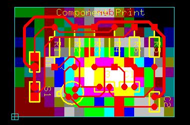
6. Color mapping of the board may be viewed by switching on the option View->Analysis Results->Colored board.
7. The analysis result is obtained. From the result it may be easy to identify the most heated up component so a heat sink of about may be used.
8. To simulate the heat sink effect, Select the tool Component Parameters and click on the component. A
Thermal Parameters window pops up where you may set the cooling parameter for the component. Check
Component Mounted Heat Sink check box, enter the Thermal Resistance of Heatsink (e.g. 1.2°C/Watt) value and click OK. Repeat the same step for all other components and execute the analysis again. You can notice the change in the isotherms after conducting the thermal analysis.
9. Labels may be placed to display the temperature at various points on the board. For this right click and select the tool
Set/ Delete Label and click on the board at required locations. Label gets tagged to the cursor. Now drag the mouse to place the label at proper place.
Note: To delete the isotherm label click again on the label.
 Electromagnetic Analyzer
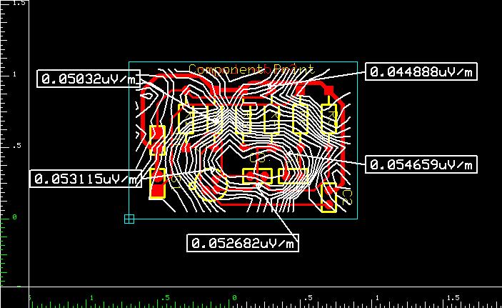
Electromagnetic Analyzer is used to predict the intensity of electromagnetic field generated by the working circuit on the PCB. An electromagnetic field develops when voltage passes through the traces on board. Once the routing of traces is complete, electromagnetic analysis may be performed on the board. The Electromagnetic Analyzer measures the distribution of the Electric Field Intensity on a finished PCB. The isolines show the distribution of the field intensity on the board. Under the electromagnetic analyzer you can perform Signal Integrity Analysis and Field Analysis.
 Steps for Electromagnetic Analysis
1. Select Electromagnetic Analyzer tab, Right click and select the tool Electrical Parameters
2. The board parameters are set to the default values by clicking the Set to default button.
3. If you select the Set to default button, the default parameter gets loaded into the text boxes. To move Net from Select Net to Currently Set Net parameters use key and to move backward use
key.
4. View the electrical parameters of the trace from point to point using the View Traces button after selecting the particular Net Name
5. After adding these nets you may execute the analysis directly. For this right click and select the tool
Execute Analysis.
The result is displayed in the form of isolines.
6. Color mapping on the board and may be viewed by switching on the option Colored board under View --> Analysis Results --> Colored Board. The analysis result is obtained. The Maximum and minimum field intensity locations can be observed.
7. Labels may be placed to display the field intensity at various points on the board. For this select the tool
Set/ Delete Isolines and click on the board at required locations. Label gets tagged to the cursor. Now drag the mouse to place the label at proper place.
 Signal Integrity Simulation
The Signal Integrity Analyzer examines the probable distortion of high-speed signals as they pass through traces on the PCB. The results of the analysis are displayed in the Waveform Viewer. The purpose is to predict how a signal deviates from its ideal (or intended) behavior in a real-world setting.
 Steps for Signal Integrity Analysis
Under normal working conditions, signals propagate from some pins of the components in the circuit (technically called Driver Nodes), through the interconnecting traces and into pins on the same or other components (called Receiver Nodes).
This analysis detects the degree of distortion of the signal from its ideal behavior while it passes through the trace and graphically presents the comparison result with the help of the Waveform Viewer.
1. Signal Integrity Analyzer is invoked from within the Electromagnetic Analyzer. Right click on the task
PCB LAYOUT in the Project Explorer to unfold a list of functions. Clicking on
Electromagnetic Analyzer in this list opens up this module.
2. Right click on the workspace and select the tool Signal Integrity
and click on any of the trace, which is to be analyzed
3. Now select a net. A window pops up where you may set all the parameters for simulation. To check the integrity of an electromagnetic signal while it passes through this trace, go through the following steps.
4. All nets are displayed in the frame Available Nets. Select a net from the list and click .The segment nodes of the selected net get displayed in the frame. Right click on any of the node and set it as driver node and another node as receiver node.
5. The electrical properties of the trace will influence the signal as it passes through it and this is shown in the respective columns. The Trace Segment parameters of the driver node may be viewed by clicking on Show Trace Segments
6. Set the following parameters.
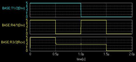
Max voltage to 5V
T L->H = 0
T H = 1us
T H-> L = 0
T L = 1us
7. Set TTL technology to the receiver nodes. Check the check box corresponding to Test Points. The Test points allow displaying the output of the selected node in the waveform viewer. If no test point is selected then output waveform alone is displayed on the waveform viewer.
8. To execute simulation, Start time and End time of the simulation as well as the sampling time interval must be specified. This corresponds to the parameters Start time, Time limit and Time step. Enter 1n for Time Step and 2µs for Time limit.
9. Click on Calculate button. The Calculate button allows to calculate the maximum time limit and will update the text box Time limit. Here the time step is set to 1ns and Time limit to 2us.
10. Check the box Generate Waveform. Click the Simulate button to process the simulation
11. The waveform obtained after simulation is shown below.
 Field Analyzer
The Field Analyzer is a tool for studying the electromagnetic fields that are created when power and/or signal traces on the board are energized. The results of the analysis may be view as a color graph, isolines, 3D-wire mesh graph, etc. It must be particularly mentioned that, just as with the other two tools, the Field Analyzer does not make any decisions or suggestions about the proper functioning of the design. The Field Analyzer predicts the variations in the selected field, due to electromagnetic properties of physical connections (traces), within a spatial area and time frame specified by the user.
 Field Analyzer - Operation
Invoke Field Analyser from Signal Integrity Simulation window.
Check the option ‘Display Fields’ in the Signal Integrity Simulation window
Click the Simulate button to open the Field Analyzer.
The Tool Box on the right side of Field Analyzer includes
 Graph Modes
The Graph mode includes
Graph Extent:
Size of the square covered in the graph can be adjust using the zoom out and zoom in button.
Select field
It includes Electric field, Magnetic field, Vector potential, Scalar potential. Output can be viewed by selecting each field.
Graph.
In this option of Field Analyzer, five types of graph can be viewed. Colored graph 


Graph Params.
Isolines density
More detailed presentation of the result can be obtained by increasing the Isolines density in the Graph Params.
Color graph:
Precision raster:
The precision to calculate the field values can be adjusted using the Precision raster.
Display grid:
Applying higher values to the Display grid will provide smoother variations to the colored graph.
 Controls

The simulation may be interrupted (and continued later) at any desired point by using the

In order to continue the interrupted analysis, simply click the 

 Plot settings
You can view the Field Analyzer Diagram by setting the parameters as your need. If Auto Scaling has been selected, the maximum values displayed as well as the scales of the graphs are automatically updated. On the other hand, if Auto Scaling has been turned off, these values are clipped at the values specified. (In other words, values higher than those specified are ignored.). Different magnetic field, electric field, vector potential and scalar potential graphs can be viewed by selecting Select Field and Graph in Graph Modes.
 Electric Field Polar Co-ordinate Graph
Fabrication Manager
 Introduction
Fabrication is the last stage of the electronic design process. The PCB information is converted into ASCII output files – GERBER (.gbr), NC Drill (.ncd), PCB Assembly Outputs Generic (.pck), IPC-D-355(.355), Bare Board Testing Generic (.bbt) and IPC-D-356A(.356) which are input to machines to finally create the hardware.
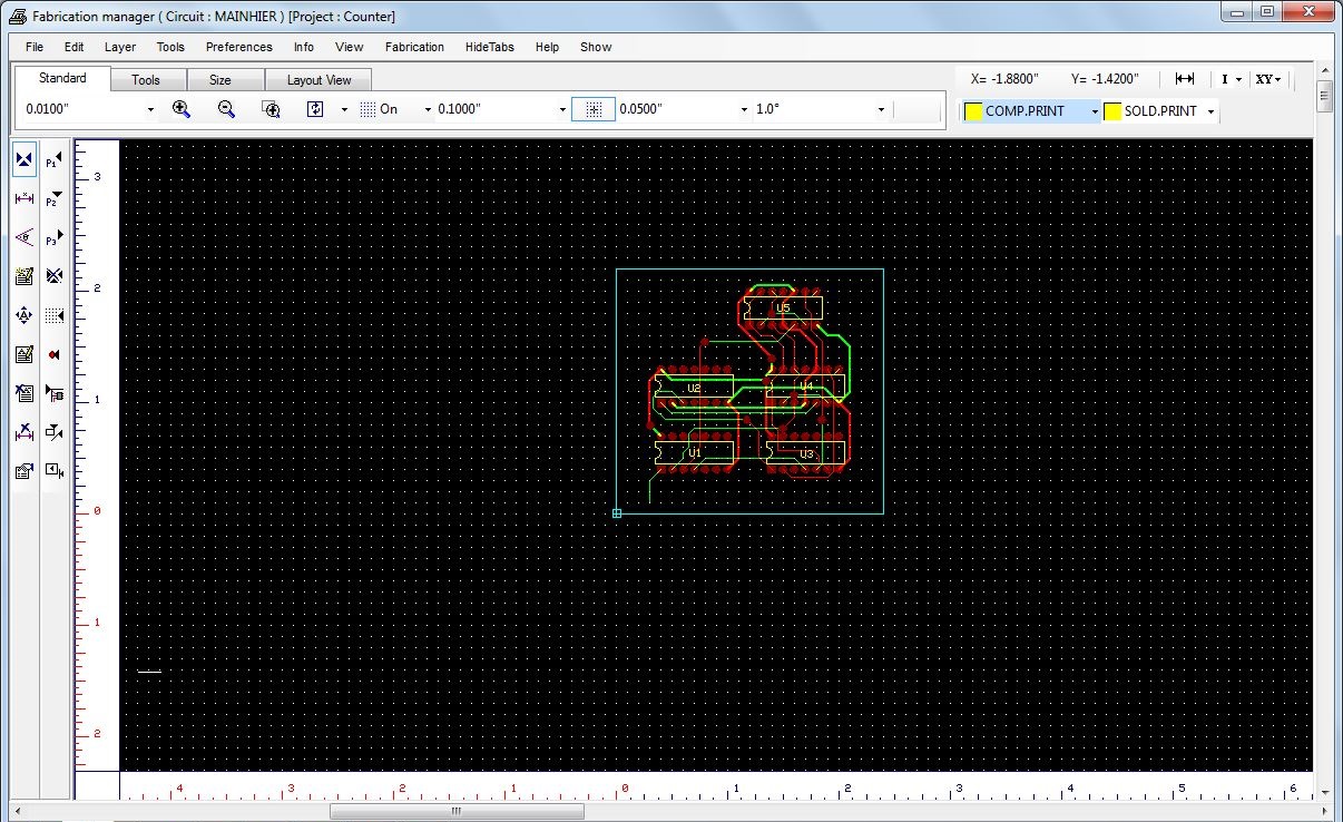
1. Invoke PCB Layout in the Project Explorer.
2. Select Fabrication Manager from the tasklist or Select from the task toolbar. The Fabrication Manager window opens with a default board size and gets aligned with the Project Explorer to fit the screen.

3. Invoke Fabrication Data Manager choose Setup from Fabrication.
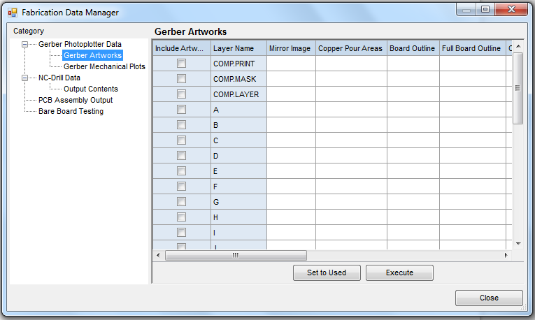
4. Choose Gerber Artworks in the left pane of Fabrication Data Manager .
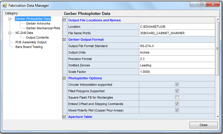
 Gerber Output
GERBER is the standard format used as input to photoplotters that generate the design data on films. These films are used as masters for manufacturing the PCB, the physical realization of the schematic data. GERBER format is a vector format for defining various elements of the layout. This format represents all traces as draw and the pads that are part of the component footprint as flashes. The Photoplotter uses this command language
1. Select the layers for which we want the Gerber Artwork files.
2. Click Execute.
3. ‘Gerber output window’ opens, Click on Execute.
4. This completes the generation of GERBER data.
 Preview the GERBER Data
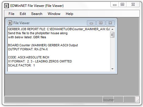
 Preprocess the GERBER file
File | GERBER Viewer Setup option. Click on Grid cell in the column GERBER ASCII File, an ellipsis (a button with 3 dots) appears, click on it and select the required GERBER ASCII files (*.GBR)..
Preprocess will happen when we select Gerber/Excellon/DXF/HPGL Viewer.A window will pop up,select a *.GBR file.A window will appear like this:
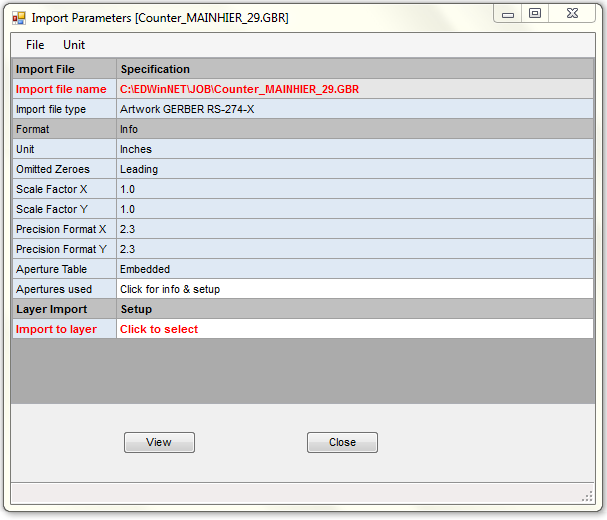
Select 'Import to layer' from the dropdown option.The preprocessing status may be displayed on the status bar and the completion is marked by a 'Successfully processed selected files.’ message. As a result, artwork file (*.ART) is created with the name of the source Gerber.
 Viewing Artwork
1. Select Artwork Viewer Setup from Gerber Preprocessor and Viewer Setup window.
2. Choose Browse Artworks
3. Select the .ART files and click on open
4. Select the files one by one and click on Apply.
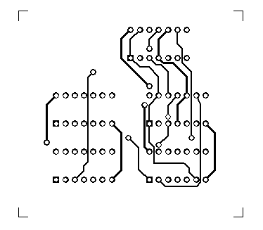
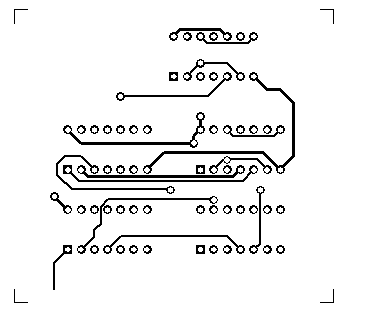
5. The Artwork of a PCB is the actual display of the various copper routes, padstack, pinholes, etc.. The design data may be viewed layer by layer as it is got on the photoplotted film or pen plotted artwork. This menu option must be active to view the various layers of the design individually.
6. Tools Artwork / Power & Gnd planes .
7. Select Define Artworks (function tool) Set Used to Accept.
8. Select Centreholes from View Artwork Centreholes as 1/3 Size.
9. In order to view layers, Select Tools Artwork & Pwr/Gnd Planes use the Layer( Comp.side & Sold.side) drop down menu and select the required layer. The artwork for that particular layer may be viewed as it appears. Select Solder Layer from tool bar.
 Gerber Mechanical Plots
This window allows setting the parameters for gerber mechanical plots on both Component and Solder side. The window opens with the Component Side, by default. Here the Generate Mechanical Plot for Component Side checkbox is unchecked. Enabling this checkbox displays the list of parameters that may be set.
1. Select Fabrication | Setup. This dialog box is shown below.
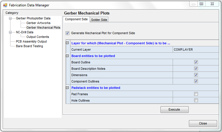
2. Click Execute, then a Gerber Output window appears.
3. Click Execute. ‘Gerber ASCII output completed’ message appears in the bottom of the window. The output obtained will be a text file.
 Introduction to NC Drill
In generating the NC-Drill, the system extracts information about the whole positions, sorts them according to drill size information. The different hole sizes are grouped together and generally sorted to drill in a specific order. This grouping may be done based on sizes, type of drilled hole, like through plated or non-plated, via type like buried or unburied etc. This is generated as a drill tape data. The data may be used directly on any numerically controlled drilling machine. This NC-Drill data is of the EXCELLON format, which is the accepted industry standard
 NC Drill Output Parameters
1. Select Fabrication | Setup | Fabrication data manager | NC-Drill Data. Depending on the equipment used by the PCB manufacturer some parameters must be set prior to generation of NC drill files.
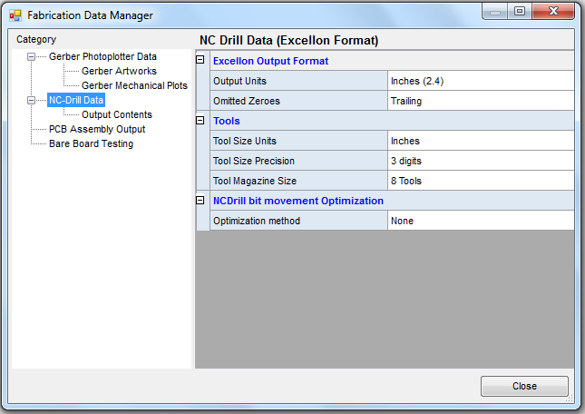
2. Set the following parameters
Output units - Inches or Millimeters.
Omitted Zeroes- Leading or Trailing.
3. Click on Execute, NC Drill Output window appears.
4. In this window check Prepare drill database for Template only and Check for multiple holes in the same XY position.
5. Click on Execute. In this window after execution displays a message ‘NC Drill Output Completed’.
6. Click Close and Accept Fabrication Data Manager.
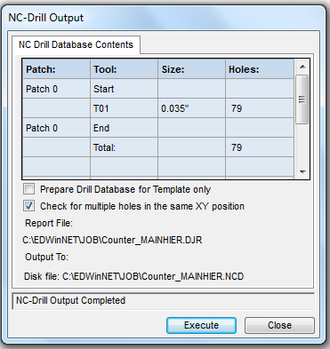
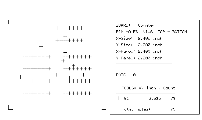
 Preview NC- Drill data:
Select Tools | Template (notes)
 Introduction to PCB Assembly outputs
When the manufacturing volumes are high and high in component density, designs like SMD, manual assembly becomes difficult. In such cases, automatic component insertion technique is required in a specified format to drive automated machinery to position the components at exact location. As this data is machine specific, there is a provision for both Generic as well as IPC-D-355 standard format of the output. Generate PCB Assembly outputs.
1. Select Fabrication | Setup | PCB Assembly Output.
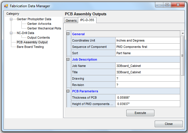
2. Click on Execute. Output is a extension .PCK extension file
3. Save it
4. Select IPC-D-355 tab on top of the Fabrication Data Manager window.
5. Click on Execute. Output is a .355 extension file, save it in the desired location.
 Introduction to Bare Board Testing outputs
Bare Board Test (BBT) is like quality check usually done by the fabricator to check the open & short circuits in and between the tracks. A supply of 50 volts is passed through the tracks and this job is done by automated machines. A probe sort of thing is inserted through the pads so as to probe. A netlist is generated from the gerber (it is not generated from the design) so that to cross check the actual physical PCB manufactured with respect to actual gerber in order to find out the fabrication errors. This is a special on board test outputs generated in Generic and IPC-D-356A.
 Generate Bare Board Test outputs
Select Fabrication | Setup. To setup parameters for Bare Board outputs choose Bare Board Testing node from Fabrication data manager choose either format and set the required parameters. Click Execute to generate the Bare Board Testing output in either Generic or IPC-D-356A format.
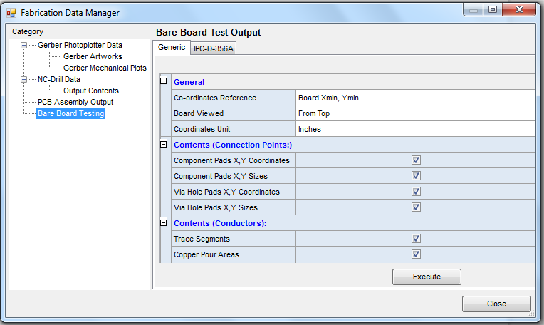
The output for Bare Board Testing is obtained as a text file.
