Introduction to Layout Design
Components are automatically loaded as a result of packaging executed while editing the schematic diagram of the circuit. Layout may be started without schematic; In that case, new parts may be loaded on the board in similar fashion as in Schematic Editor. Location and orientation of components is defined either by manual relocation to desired position, using coordinates or with the help of auto placer. Traces may be routed manually with automatic via insertion whenever routing layer is changed. Sixteen types of user defined via pads are supported. Layout Editor also includes a number of online automatic functions to route/ reroute traces for single nets and to reroute existing traces for relocated components. Dedicated full board auto router and import /export interfaces are also integrated with PCB Layout Editor. Copper pour areas are defined as polygons and may be placed on any trace layer. Insertion of air gaps and thermal pads on artworks is automatic.
Design rules for manual, semi-automatic and automatic routing of traces and component placement are user defined and may be set individually for each project. Design rules violation, clearance errors and missing or incomplete connections are detected automatically.
The Design rules for the project may be set in the Project Design Rules window. This may be launched by Project Explorer | Project | Project Design Rules (Refer page: 76).
Configuring the Editor
Board ConfigurationDefault board formats for the workspace may be set in the Project Explorer | System | Options window. The user can select pre-defined formats or create own formats. It is advisable to set the required board size to avoid unnecessary wastage of space.
Features
- Maximum board size available - 4m x 4m.
- Maximum number of layers on board – 32 (28 trace layers, 2 silk screen & 2 masks)
- Available page formats – American & European.
American formats: AA , AB , AC , AD , AE , AF
European formats: EA , EB , EC, ED , EE , EF
By default American format AA is enabled.
Starting of Layout Editor:
This module may be invoked from Project Explorer in the following ways.
• Right click PCB Layout and select Edit PCB Layout from the list or Double click PCB layout
• Select Edit PCB Layout from the main window.
The Layout Editor menu description is as explained as below.
Layer
Allows to select the layers on which the trace is to be routed the text is to be placed or Copper Pour Area is to be defined. The trace may be on any selected electrical layers. Each layer can be set to different colors in Project settings to differentiate between the layers.
E.g.: Default settings for Comp layer: Green color.
Tools
Displays a list of menu items that is present in Schematic, Layout and Fabrication Manager. The menu in this list differ in each editors and when selected allows entering into main object oriented function.
Tools(Components)
Enables component editing mode, presenting various tools that performs operation related to components.
Tools(Connections)
Enable connections editing mode, presenting various tools that performs operation related to connection between the components.
Tools(Texts)
Enable text editing mode presenting various tool that performs operations related to text
Tools(Block Edit)
Enables Block editing mode and presents various tools that performs operation related to objects like components/ wires in block.
Tools(Board Outline)
Enables Board outline editing mode presenting various tools required to perform operations related to editing the default board format.
Tools(Autoplace)
The tools required for autoplacing are displayed on the workspace when Tools| Autoplace menu is invoked.
Tools(Copper)
Edit Copper function enable to place conductive elements on trace layers. Conductive elements may be either of the graphic items (Copper planes) - Lines, Arcs, filled and unfilled Circles and Rectangles or a new type of item - Copper Pour Areas.
Copper planes are solid copper blocks where air gaps for pads/ traces may not be created. Such copper planes are usually used for shielding and as Keep Off Zones. It is recommended not to use these copper planes for distributing power supply or ground since Copper Pour Areas may be used for such purposes. In some cases, it may be necessary to relieve certain areas on the board from copper. This may be done by creating Copper Pour Areas in any shape. At least three vertices must be defined. This will relieve copper on the processed layer.
Tools(Via Padstack)
A dialog box Edit Via Padstack lists all the layers supported by the system. Selecting any layer highlights the other parameters associated with the padstack. The hole diameter may be specified in either inches or mm and the shape toggled between round and square. To make any changes to the default values, click on the necessary layer. The particular cell becomes editable. Enter the necessary values and click. To change the shape, click on the particular cell and select the shape. Click on ACCEPT to save the changes made.
Tools(Bury Vias)
Selecting this menu pops up a confirmation box to confirm burying the vias. On clicking YES, Buried Vias Layer Sandwich map dialog box opens. This dialog box provides information regarding vias present in the loaded database. Click ACCEPT button. The vias will appear only on the intermediate layers enclosed by the layers between which the electrical connectivity is made.
Tools(Unbury Vias )
When enabled, it simply unburies the vias. This implies that the vias will now be visible on all layers except on Comp. Print and Solder Print.
Tools(Characteristics Impedance Calculator )
Calculator is a tool to plan PCB stack up to achieve controlled impedance. It allows designing layer stack (from available EDWinNET layers), assigning layer type property (PWR/GND, Signals or Mixed) and other parameters (dielectric material, thickness of dielectric material, Cu thickness and trace width on signal layers).
Program automatically applies suitable characteristic impedance formula depending on layer configuration. (Microstrip, Stripline and Dual Stripline). It is also possible to calculate required trace width, Cu thickness, thickness of dielectric, and permittivity for the layer when value of characteristic impedance is specified as a design rule.
A common dielectric materials Library is integrated with calculator. Entries in this library may be edited by the user and new materials added.
Tools(PCB Wizard)
Preferences
Preferences (Active Layers on Top)
Allows displaying the active layer selected as the top layer, giving it priority over the other layers.
Preferences (User lay prefix)
Allows changing the component name prefix.
Preferences (Stacked Layers)
Allows displaying all the active layers stacked one above the other.
Preferences (Display Traces in XOR mode)
Toggles the display of traces in XOR mode.
Preferences (Auto Connect Settings and lists)
The execution of auto-connect functions may be controlled by setting different options in this dialog. It also contains lists of components currently scheduled for re-routing and list of currently routed lead-outs.
Preferences (Online Trace Clearance Check)
Displays if there is errors after routing the trace.
Preferences (Tear Drop pads)
Pops up a window Tear drop auto generation where the options (size and shape of the tear drop pads) for Tear drop generation maybe set.
Preferences (X /Y/Z Coords)
Allows determining the current cursor position with respect to a given reference point in terms of the X, Y and Z coordinates. The values are displayed in the position toolbar.
Preferences (Lock Toolbar)
Anchors all the toolbars at the placed location.
Preferences (Meshed Copper Pour Areas display)
Enables to view the meshed copper pour areas present in the layout.
General Options
Preferences (Guidelines (Net))
Allows displaying a single ratsnest associated with the selected net while routing or relocating a trace
Preferences (Guidelines (Next Unconnected Node))
Allows displaying the next unconnected node of the net while routing or editing.
Preferences (Ratsnest for unconnected node only)
Allows toggling ON/OFF the display of ratsnest of unconnected nodes only.
Delete unnamed nets when connection is deleted
This option when enabled will delete nets that are not named if the trace is removed.
Preferences (T-connect Same Net Only)
Allows T connections to be made only on the same net while routing traces.
Preferences (Inherit Trace width from T Connection)
Inherits trace width from T Connection while routing new traces.
Preferences (Reroute component connections after Move)
The option serves an important purpose of automatic reconnect the nodes of a component if the component is relocated or swapped.
Preferences (Auto taper after routing)
If tapered is set, any trace segment may be assigned different widths at the start and at the end. If the width at the end of a segment is smaller than at the beginning, then the segment will taper down gradually along its all length. In opposite case, such a segment will taper up from smaller to bigger width. This function also creates smooth change of width in cases when thicker trace must be routed between pads.
Preferences (Center)
Allows setting the origin coordinates to the Center. The co-ordinate information displayed in the position toolbar is with reference to a point on the board. This defines the center of the board as reference point for all coordinate and dimension information.
Preferences (Board Datum)
Allows setting the origin coordinates to bottom left corner of the board.
Preferences (Refpoint)
Allows setting the position of the origin coordinates on the workspace with respect to a reference.
Auto
This drop down menu allows performing automatic function such as placement, fanout and renumbering of the components in the circuit, routing of traces etc in the most optimum manner. It also allows setting layers for the clearance check.
Auto(Autocheck)
Clearance Check Setup dialog box allows to set up clearance parameter value, Other DR Violations tab in this window is used to set other clearance check parameters and Global test report tab allows to execute all available tests in proper order and produces test report containing details of all detected problems.
The Parameters include
• Pad to Pad distance
• Pad to Trace distance
• Trace to Trace distance
• Channel width for single trace check
Also allows toggling ON/OFF the layers on which the check is to be performed. After proper setup of the values, the system is ready to perform Auto check on the board.
Auto(Autorouter)
Allows routing the current Project automatically by selecting any one of the three autorouters available. The three menu items listed under this are:
• Autorouter - Arizona
• Autorouter - Specctra
• Autorouter - Maxroute
Arizona Autorouter
Arizona auto router is an integrated module of the EDWinNET. It uses its own temporary project and simplified graphics. The Arizona auto router allows routing the traces of a PCB Layout automatically. The netlists is given as the input to the auto router. When this router option is selected, all non orthogonal traces will be removed and accepts only orthogonal traces as prerouted traces.
Various options such as load Pre routed traces (only orthogonal traces); load copper setting layers etc may be set before autorouting. With these options set, system initiates the routing process. The original project is visible in Layout editor until you update the main project from the autorouter.
SPECCTRA Autorouter
SPECCTRA auto router is an integrated module of the EDWinNET and is designed to handle high density printed circuit boards that require complex design rules.
SPECCTRA autorouter uses powerful Shape Based algorithms to make the most efficient use of the PCB routing area. The results are high completion rates while following high speed electrical rules.
SPECCTRA conserves system resources by not using memory consuming grids. It handles staggered pin components and routes through them with ease. Its diagonal routing algorithms, operating in either grid or grid less mode, handle components of non-standard dimensions that previously required manual routing.
MaxRoute Translator
The MaxRoute Translator is an application that allows converting layout project (database) to a form that is acceptable to MaxRoute Autorouter and MaxRoute Autoplacer. It outputs all the information necessary to reconstruct the system layout project (database) in MASSTECK. This module may also be used to import routed traces from MaxRoute Autorouter as well as results of MaxEDS Autoplacer.
Auto(Autofanouts)
Provides option to setup selected net fanout parameters and generate fanout on the board. SMD pads may be connected to copper pour areas (ground or power supply) in following manner:
1. Copper pour on Component or Solder side layers if the component is placed on this side of the board.
a. Pads may be soldered directly to copper.
b. Pads may have heat relieve items in the pad stacks, which must be shaped in such way that they provide proper through pass from copper to pad
c. Pads may have a trace stub with air gap = 0, which will provide conductive bridge over pad’s own air gap to surrounding copper. This type of connection is called fanout without via hole.
2. Copper pour on middle layers.
3. Pads are connected to copper by short trace stubs terminated by via hole. Via holes provide necessary connection to copper underneath. This type of connection is called fan out with via hole.
Auto(Autorenumber)
When a schematic is converted to a layout, the placement is governed by shortest length of connectivity, ease of routing, functional organization etc. After completing the layout, it is necessary to order the components to aid manufacturing stage at the assembly shop and to help ease of testing.
Autorenumber allows re sequencing the components on the layout in a specific order by setting the given parameters in the dialog box. Component prefix and starting number may be entered with respect to certain parameters such as board corner, coordinates, directions etc. Channel width may also be specified. Click ACCEPT once the selection is complete.
If the component prefix given in the dialog box is not matching with any of the components in the loaded database the system issues an appropriate error message.
Auto(Net Trace Integrity)
Ensures that project integrity has not been corrupted. In rare cases the internal cross references between objects in the project (database) may get corrupted. It may cause malfunctions of the system. This function performs test of internal cross-references. If some references point to missing objects then the referencing object is deleted from the project (database). In most cases objects containing references to missing object cannot be deleted any other way because they are invisible on the screen. It is useful to execute this function from time to time to ensure that project (database) integrity has not been corrupted.
 Parallel Routing
Working
- From Auto menu in Layout Editor, select Parallel Routing option. This will enable the Parallel routing mode. Enable Connections – Route.
- Earlier for Parallel routing of traces depress the key combination Shift + E prior to selecting a starting pad of a traces set. This enables the mode for blocking several pins. Selecting the pins will enable parallel routing window where you can specify the routing space. Specify the spacing and click on Accept button.
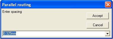
- The pad that is closest to origin of the blocking rectangle is taken as starting point of the leading trace in parallel group. The leading trace may be routed and other traces will follow it parallel with specified spacing.
- After arriving to final destination for the leading trace, it can be connected in normal fashion. When leading trace is connected, the next unconnected is taken as the leading and parallel routing continues until all in the bunch been connected or operation aborted by ESC
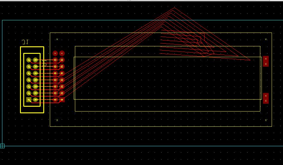
- In some instances, it may be needed to narrow the spacing between traces to get through a tight spot. In such cases, routing of the leading trace and parallels may be terminated at any point with F4 key. With option “Allow T- connections” ON, lose ends of previously routed parallels may be grabbed in similar fashions as pads by blocking and new spacing (smaller or bigger) is applied.
 Interactive Routing
Working
- Enable Connections in Tools menu, select Route from Connections. Then select Interactive Routing option from Auto menu.
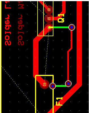
- Select the pins of required components and click and drag it (earlier it has done by Shift+A) as shown below
Info
Info(General)
Opens a dialog box where information regarding the objects placed in the workspace may be obtained.
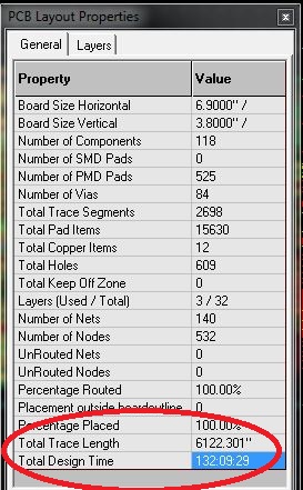
Total Design Time
The total design time has been added to the Statistics menu.
Working
- Select Statistics from Info menu in Layout Editor. A window will pop-up as given below
Info(Statistics)
Pops up a PCB Layout property window that displays all information related to the board such as board dimension, number of components, pads, holes for pins, via holes and total holes etc.
This also gives information about the layer usage such as layer name, number of trace segments, pad items and copper items in each layer.
Info(Buried Vias)
Opens Buried Vias Layer Sandwich map dialog box that allows display of information on the buried vias used in the loaded project. If no buried vias exist, a message box displays buried vias not found. If there are any buried vias in the layout, the layers sandwich Info is displayed, which shows the number of buried vias and the layers on which they are created. A cross mark placed against a layer indicates that a buried via exists in that layer.
List of Copper Pour Areas
Gives information on Copper pour areas in the circuit.
Steps to follow to define board outline
i. Select
Board Format from Tools toolbar.
ii. Select the function toolDefine Outline.
iii. The option toolCreate Board will be enabled. This tool enables free hand drawing, using which a board of desired shape can be drawn on the workspace.
iv. To select a pre-defined board format, select the option toolTextual Mode. The Properties Board Outline (Create) dialog pops up as shown in Fig.8.1.
v. Enter the desired values and click ACCEPT button.
Fig.8.1
Loading components
This section deals with how to extract components from the
respective libraries and position them on the layout editor. The components
placed on the schematic, which contain both symbol and package, are front annotated
to the layout after packing. These components are positioned at board datum
(0, 0) automatically and can be relocated either manually or automatically.
If new parts are required to be added, they may be extracted as part using options
of the function tool
Open part library.

Components can be loaded in the working area using any one of the following four ways:
i. Component Browser
ii. Using Library Explorer
iii. Using Library Browser
iv. Add Components
Select
Open part library function tool to display the last three option tools.
Placing the Component in Layout
This section deals with the layout creation of Half Adder. All the components for the Half Adder is already packed from the schematic (refer page 142), so they are automatically front annotated to the layout and will be positioned one above the other at the board datum. The netlists information will also be updated simultaneously, which make the routing easier.
Before we start loading Parts on to the page, turn ON Grid
by enabling grid from the dropdown,
in Standard Toolbar. The value for grid may be selected from the drop down list
as .1000”. Similarly, set Snap value to .0500” for better placement
of the components.
Select
Components from toolbar and right click on the workspace to popup a set of Component
editing tools. By default this tool is invoked with the
Relocate Component tool enabled.

The components may now be relocated in the following way.
1. Click on the component .A confirmation box pops up to show the selected component. Select YES if the selected component is U1 or else select NO till U1 is selected. Move cursor to a position well within the board to place U1. To orient this component by 90? / 180? / 270? on the board, click
Rotate Component by 90 degree tool or press F1 key to rotate the component until it is in the required position. Press F1 3 times to place the component as shown below. Click mouse to place the component. Select the function tool
Relocate the Component by name and place it below the component.

Relocate Component function tool to view ratsnest while relocating the
components to ensure that components having a large number of interconnections
are positioned close to each other. Pressing SHIFT key while relocating/ stretching
an item allows the item to move/ stretch smoothly.
2. When a component is being relocated, all other component placed at board datum will disappear which reappears on
Redraw.
3. Place U2 and J1 in the same method described above. Final placement should appear as shown in Fig.8.2.
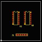
Fig.8.2
Next topic guides you through routing the PCB board.
Routing the Board
Connections between components may be established by using
TRACES and COPPER POUR areas. Click
Route from Tools toolbar to enable a set of Routing tools on right clicking
the workspace.

Adjust zoom precision to view the pins properly.
Turn on Preference/ Guidelines (Next unconnected node) before routing because
this option guides you to take the easiest path to route.
Select True Size and Pad frames from View/ Layout, enabling you to select proper
trace size. This also prevents you from creating errors such as traces crossing
over pad, traces very close together etc.
First route power and ground signals (Net SPL0 and +5V). In Project Explorer,
select Project / Project Design Rules and set the routing width to 0.030”
for Pwr/Gnd lines and 0.013” for Signal lines.
To start routing traces, first select the power points; say pin 14 of U1 and
route to pin 14 of U2.
The steps to complete this connection are as follows.
The trace connection may now be created in the following way.
1. Right click and enable tool
Route to start routing connections. Select layer for routing from Layers in the main menu. 28 layers are available for routing. By default COMP LAYER is selected. Click on pin 14 of U2 to route on SOLD LAYER. A small triangle appears at this pin and cursor changes to a crosshair with a square. The next node in that net is displayed with ratsnest ending with a rectangle as shown in Fig.8.3.


Toggle arc insert (F11) to change routing directions in arcs.

Fig.8.3
2. Move cursor with 45° angle through a short distance and click at the nearest point as shown below. The first segment has now been anchored. Now take this trace horizontally and click near 14th pin of U1. Once again take bend point at 45° angle and connect the trace to 14th pin of U1.

Fig.8.4
3. Terminate routing of the trace by pressing END or F4 key on your keyboard. Or click on the tool
End Connections.
4. Connections of 5V net have been accomplished by traces. The Ground net connections can be done by using a copper pour area. Select
Copper from the Tools toolbar. Select the second Function tool
Create Copper graphic item and select the fifth option tool
Create copper pour area. Now select the net to which the copper pour should belong by selecting SPL0 from the dropdown list box
in the Sizes toolbar. Now start creating the copper pour polygon by clicking near the 7th pin of U1. Clicking on any point introduces a vertex at that point. Enclose the 7th pin of U2 and the entire connector, then right click and press
Finish Copper Pour Create.
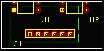
Fig.8.5
5. Semi-autorouting functions can also be used to route connections. Select the function tool
Auto Connect Traces. Select the first option tool
Auto Connect Node Pair and click on the 2nd pin of U1. A rubber band like connection shows where it has to be connected as shown in Fig.8.6.

Fig.8.6
Click on the node where the rubber band connection ends, i.e. pin2 of U2 and the connection is automatically routed, now press
End Connection.

Fig.8.7
6. Uses the second option tool
Auto Connect net to autoroute a net. Click anywhere on the workspace, an input box appears, enter the name of the net, which has to be routed, say A. Clicking on a node belonging to the net A will also achieve the same result (i.e. clicking on pin 1 of U1).
7. Repeat the same procedure as in (5) for the nodes at pin 3 of U1 and U2 respectively as well as the rest of the unconnected nodes on the connector.

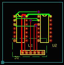
Fig.8.8
To avoid errors
1. While routing, click on pins and then enable the tool
Pin to pin. This will allow routing between pins and ensures proper connection.
2. Routing between pads should be done carefully, else trace connections get merged to the pads thus producing errors. This may be avoided by enabling True size ON from View menu, thus while routing the board; trace-pad distance may be noted and changed.
Assign Nets
Entry points having electrical connections in schematic are highlighted as nodes in the layout. Net is a collection of nodes that are electrically connected together. The creation of a trace automatically results in creation of the corresponding Net. A trace is merely a visual representation of the corresponding net description.

Creating Nets
User can create a Net connecting the desired entry points using the available tools. The system by default assigns name to each net (E.g. UN1, UN2 etc. - UN stands for UNNAMED) and these may be edited or renamed according to user’s convenience.
Net Names
The default net names (UN1, UN2 etc…) assigned by the system may be renamed according to the function it performs. System allows naming the net as PWR/GND, NAMED (RESET, CLOCK…) and UNNAMED nets (UN1, UN2....).
Advantages of using Net names:
i. Editing the nets in complex project becomes simpler.
ii. Net names indicating the function makes job easier in identifying the nets and is helpful while simulating the circuit.
iii. The other advantage of NAMED nets is that while working with complex circuit, a different designer would come to know the status of the net to be NAMED net, so that this information prevents that user from tampering the net name.
Default Nets
The power and ground pins are assigned to the part at the time of part creation. These are referred as SPL1 and SPL0 respectively and are called the Default Nets. After packing components in the schematic, these nets are automatically represented as nodes in the layout.

Net Priority
Priority is first given to PWR/ GND, then NAMED nets and then to UNNAMED nets. While merging, when a NAMED net is merged to UNNAMED net, the resulting net has the name of the NAMED net. In the same way, when a PWR/ GND net is merged to NAMED net, the resulting net has the name of the PWR/ GND net.
Incase of nets having the same priority, the second net selected gets merged into the first net; i.e. if two UNNAMED nets UN1 and UN2 are to be merged, and if UN1 is first selected and then UN2, the resulting net has the name UN1.
Autoroute Traces
A set of tools has been provided to automatically route the traces between selected nodes and selected net. Autorouting can be done by either using the function tool Autoconnect Traces or by using any one of the three available autorouters.
How to route using the function tool?
i. Select the function tool
Autoconnect traces.
ii. To autoconnect selected nodes of a net, select the option tool Auto Connect Node Pair. Click on any node of a net. The trace gets connected to the node and remains tagged to the cursor showing a connection to the next nearest node of the selected net. Move the mouse to the next node and continue this process till the last node of the selected net is connected. END key completes the current routing action. This is a semi automatic process.
iii. To connect a selected net, select the option tool Auto Connect Net. Click on any node of a net. A confirmation box pops up confirming the route. Click Yes to route the trace. All nodes of the selected net get routed.

How to use Arizona Autorouter?
Select Auto?Autorouters ?Arizona from the Layout editor menu bar.
The function toolbar of Arizona autorouter is explained below:
Parameters setup
Routing Parameter Setup
This option pops up Routing Parameter Setup to set routing directions for the selected layer, set clearances between pads, vias and traces, setup routing scheme and wrong layer cost for the design, to set trace width & to select via padstack for Pwr/ signal connections, set fanout routing parameters, setting optimize costs parameters such as Trace right direction, Trace wrong direction and Vias. Toggle ON/OFF routing of Pwr and/or signal connections. If the settings in Default Design Rule dialog is to be used, then enable the options provided.
Routing net parameters
This option pops up Net Parameters to set routing parameters for individual nets & net groups. Click on each net to pop up Design Rule set dialog where the necessary options may be set.
Interactive routing
Selected pad pair
Option to route traces for selected pad pair.
Delete & reroute selected trace
This option tool allows deleting a single trace and rerouting it again.
Selected component
This option tool allows to route all traces connecting selected component.
Delete traces of selected component
Option to delete all traces connecting selected component. With this tool selected, click on the component whose trace connections are to be removed. All the routed traces of that particular component get deleted immediately.
Fanouts for selected component
Option to preroute fanouts for selected component. Select this tool and click on the component whose fanouts are to be prerouted. The escape wires for the components gets prerouted.
Fanouts for selected net
Option to preroute fanouts for selected net. Select this tool and click on any of the nodes of the net whose fanouts are to be prerouted. The escape wires for all the pads in the net gets prerouted.
Fanouts for selected SMD pad
Option to preroute fanouts for selected SMD pad. Select this tool and click on the SMD pad whose fanouts are to be prerouted. The escape wires for the selected pad gets prerouted.
Auto routing routines
Fanouts on whole board
This option tool allows to preroute fanouts for whole board. When this tool is selected, the escape wires for all the components (for the entire board) gets prerouted.
Start autorouter
Option to start router in full auto mode. This option tool when selected starts the execution of the autorouter. Routing is done according to the settings made. The status bar shows the percentage of completion of the routing.
Remove redundant vias
Option to remove redundant vias. On selecting this tool, the redundant vias are removed and the whole trace gets re-routed in a single layer.
Clean up
Option to clean up the design after routing. After routing, selecting this option tool optimizes the layout project by deleting the unnecessary trace loops or trace segments, which have been created.
Test for conflicts
Option to remove clearance and route rules conflicts. Select this tool after routing. The number of traces tested and number of traces found OK. Are shown in the status bar at the bottom. In case any contrariety is found with the traces, they are removed. The traces thus removed can be identified using the tool Display list of unrouted pairs. The routing may be done anew to get rid of the contrarieties.
Optimize
Option to optimize routed results taking into consideration, the optimization cost parameters and the weight of the traces, which result. During optimization the router tries to reroute every trace and if it gets weight of new trace less than previously routed then it deletes old trace and puts new one to the project, otherwise nothing to be done.
To remove as much vias as possible 'Via Cost' should be setup as at least 1000.
List of unrouted pairs
This option tool displays the list of unrouted pairs in the design. This option tool when selected pops up a dialog box listing the unrouted pairs. The copy screen to clipboard button may be used to copy the list of unrouted pairs in case it is required for say, verification purposes.
Miter
Option to miter all orthogonal traces & finish autorouting. When this tool is selected, a dialog box pops up to confirm the mitering operation because once it is executed; re-entry to the autorouter is not allowed.
How to use SPECCTRA Translator?
From the Layout Editor, select the menu Auto | Autorouter | Specctra.
The Specctra Translator window is as in Fig 8.9
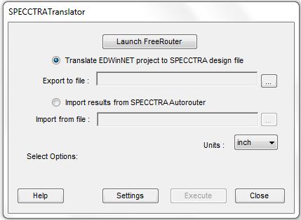
Fig.8.9
Translate project to SPECCTRA design file
Using this option the currently loaded project (database) can be converted to be compatible with SPECCTRA design file format. Before translating the project (database), the parameters for trace widths, vias and grids, the clearances and the trace type to be routed on the layers etc. are to be set. This can be done using setup from the menu bar.
Import results from SPECCTRA Autorouter
Using this option the SPECCTRA Autorouter results stored as SPECCTRA Routes files (with extension .rte) may be imported to the current project (database). The traces in the current project (database) will be replaced by the imported results. On clicking EXECUTE, a confirmation box pops up to confirm that the traces may be replaced.
Import results from SPECCTRA Autoplacer
Using this option the SPECCTRA autoplacer results stored as SPECCTRA Place files (with extension .plc) may be imported to the current project (database). On clicking EXECUTE, a dialog box pops up to select the required Place file. The components will be relocated as per the positions specified by the imported file.
How to use MaxRoute Translator?
From the Layout Editor, select the menu Auto | Autoroute | Maxroute.
The Maxroute Translator window is as shown in Fig.8.10
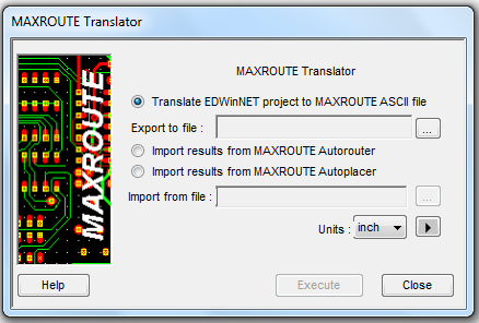
Fig.8.10
Translate Project to Maxroute ASCII File
This option allows to translate the currently loaded project (database) to MASSTECK ASCII file (files with .MIN extension) that are acceptable to Maxroute Autorouter and Maxroute Autoplacer. This file includes pad code assignments, packages, copper areas and layout texts, which will be treated as keep-out areas.
Import Results from Maxroute Autorouter
This option allows importing the results of Maxroute Autorouter back to the system. All traces in the current project (database) will be replaced by imported results (routed traces) from Maxroute Autorouter, which are stored as MASSTECK ASCII files with the .MIN extension. The file to be imported should correspond with the currently loaded project (database).
Import Results from MaxRoute Autoplacer
This option allows importing the results of MaxRoute Autoplacer back to the system. All components in the current project (database) will be relocated according to imported results from MaxEDS placer and stored as MASSTECK ASCII files with .MIN extension. The file to be imported should correspond with the currently loaded project (database).
Properties of a trace
How to invoke property window and edit properties of trace?
Select (bullet) the object (trace) first and right click on the trace. In the pop up menu, choose Properties/Trace to display the property window as shown in Fig.8.2.
Net Width . Gap Layer |
Displays the net name. The width of the trace segment may be changed here The airgap size may be set using this field. Allows to select the placement layer for the text |
Fig 8.11

The common parameter changes related to different traces (when more than one traces are bulleted) such as trace width, airgap and layer name may be changed from this panel. To do so, click on Traces in the left windowpane to display these parameters. Against these parameters, change the sizes/ select the layer. The individual trace and segment parameters may be viewed/ changed by clicking on the respective trace/segment found on the right pane in this property window. The segment parameters include width, airgap and placement layer, which may be changed or its position and length of the segment may be viewed.
How to invoke property window and edit properties of net?
Select (bullet) the object (net) first and right click on the trace. In the pop up menu, choose Properties/ Net to display the property window as shown in Fig.8.12.
| Name | Displays the net name that is mandatory. |
| Status | The status of the net may be set to either Power/ ground, Named & Unnamed. |
| Trace width | The width of the trace segment may be changed here. |
| Air gap | The airgap size may be set using this field. |
| Layer Name | The placement layer of the trace segment may be selected. |
The common parameter changes related to different nets (when more than one traces are bulleted) such as status, trace width, airgap and layer name may be changed from this panel. To do so, click on Nets in the left windowpane to display these parameters. Against these parameters, change the sizes/ select the layer. The details regarding the pins of the same net are displayed by selecting each pin under each net name. The parameters that may be viewed are Layout component name, Pin number, Connected or not, Schematic component name, Schematic entry number, found in schematic page.
Testing the Board
While designing a PCB, it is obvious that a number of errors may occur. These errors may be in the form of overlapping pads, unconnected NODES, traces crossing another trace, etc. Such errors must be taken care of before printing the PCB. To find out such errors, certain checks on the board. Connectivity and DRC check are two methods by which the errors may be generated on the board and using the necessary tools, these errors may be rectified.
Fig 8.12
Connectivity Test
Connectivity test may be used to check whether there is any electrical discontinuity (unconnected nodes or deleted trace segments) in a single net. By setting certain parameters, the test can be performed either on individual nets or all the selected nets. It can also be specified whether to stop the test and display the results when the first discontinuity is encountered or to continue the test for all nets even if discontinuities are encountered and display the entire results at the end.
How to perform Connectivity Test?
i. Select
Connections from Tools toolbar.
ii. Select the function tool
Connection Property, select the option tool
Test Connectivity and click on the board or on a net. The Connectivity Test dialog pops up.
iii. Select the required nets using the move keys and click the connectivity test tab.
iv. Under Connectivity test tab, set anyone of the three options:
• Stop at first fail: Test stops at the first occurrence of error.
• Test all selected Nets: Checks whether all NODES of the selected NETS are connected.
• Test single Net: Checks connectivity of the NODES of the selected NET.
• Click the TEST button to display the results
v. Perform this test until “Tested Nets – Fully Connected” message is displayed in this window.
Design Rule Check (DRC)
This utility is used to create an error free board to enhance the efficiency of your board. It automatically smoothes, miters, and checks for both aesthetic and manufacturing problems that might have been created in the process of manual or automatic routing. Number of design violation parameters may be used to verify the layout of a board. Layout conducts a design rule check with the parameters checked and any problems are marked by an Error label and may be queried using the Redraw/ Error. The design rule settings may be saved as a permanent setting or may be set for the circuit or for the current project only.
This test helps us to check the clearance between pad to pad, pad to trace and trace to trace.
How to perform Design Rule Check?
1. Select Autocheck from Auto Menu. The Auto Check Setup dialog pops up as shown in Fig.8.14.
2. Select the layers and enter the clearance value in the window. To select all the layers used in the project click the SET TO USED button.
3. If any Design parameters are used for the project then check Use Clearances as in Design Rules. Click on Check other DR Violations tab and set the required options. For more information on this please refer main help.
4. Click EXECUTE.
Fig 8.13
After selecting the layers from autocheck menu, follow the steps given below:
1. Select
Block Edit tool from Tools toolbar.
2. Select the first function tool
Check Clearance in Block and draw where the clearance has to be checked. To test clearance for the whole board use its option tool
Check Clearance on whole Board and click on the board.
3. System displays a label ERR# to highlight the type of error, it had encountered. The following are the error number generated:
• ERR1- pad too close
• ERR2- pad on pad
• ERR3-pad/trace/items too close
• ERR4- pad on trace items
• ERR5- trace/ item too close
• ERR6- trace/ item x-ing(crossing)
• ERR7 – Shortcuts to copper pour:
• ERR8- non orthogonal trace
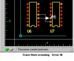
The color of the label ERR# indicates which layer the error is located. The encountered type of errors may be viewed using the menu View/ Errors/Display errors. The statistics may be obtained from the menu Info/ Errors.
Following is an example of ERR labels generated after an autocheck is performed on the board.
Board Analysis
Various factors like component placement and routing may influence the working of the circuit. Different types of analysis may be performed on the designed PCB to find out how these factors influence the functionality of the circuit. There are plug-in tools like Thermal Analyzer, Electromagnetic Analyzer and Signal Integrity analyzer for analyzing the thermal, electromagnetic and signal integrity effects on the board.
Miscellaneous
Layout Package
Generally, layout packages are formed as a result of packaging of symbols in the schematic editor. If necessary, new packages may be created and added to the circuit while editing the layout. If this is to be on the schematic diagram, the part added must have both the symbol and the package.
Part description contains all information about layout view (package) and schematic view (symbol(s), packaging and pinout) of the component. There are also parts, which do not have symbol information prohibiting them from taking part in back annotation.
Parts, which do not have symbol, are not back annotated to Schematic, but part containing both symbol and package is back annotated to the Schematic.
Layout Component as ‘Package’
It is also possible to create new layout components using only packages as reference but referred as parts. In this case no information of symbols will be passed to schematic diagrams. One of the main purposes of this mode is to create layout components, which are not required to appear on the schematic diagram. For e.g. it may be needed to reserve space for screw holes in the PCB board as shown in Fig.8.15.

There is no explicit function to create holes for fixing screws. A package may be created or an existing package used whose pads represent holes while generating NC drill list.
{bmct tmp1.bmp}The component(s) placed by either of the tools (Browser/ Explorer) has component name (E.g.: U1) displayed by the side of the component.
Selecting Objects
Refer selecting objects in Schematic Editor Page
Change reference
How to change reference?
Purpose: To change the reference of a component placed on the editor.
Operation: Open the Library Browser or Explorer and click on the component present in the search list. Press Alt key and drag the component from the Browser or Explorer to the editor and move anywhere over the component, which is required to be replaced. Now, release the mouse. The reference of a component may also be changed in the following way: Select (press Ctrl and click on the component) the component and right click anywhere on the workspace. A menu pops up from which click Properties/ Layout Component Property window pops up where various option are provided for the bulleted component(s) and its entries. To change the reference, type the required Part name in the Part field. Press enter or click the next row. The part on the schematic editor is replaced if the component name typed is available in the Library.

Renumber Components
After the PCB layout design is complete, it is a normal practice to renumber the components. This is required, because, while placing the components on the board either manually or automatically, the optimization of connecting length is the governing criterion. However, for the board to be assembled and serviced, it is desired to have an orderly sequence in component naming. There is an automatic function to perform this. The numbering sequence may start from the top of the board, move in an ascending order to the right in a row, or start from top, and then move down in a column like:
| ROW ORIENTED | COLUMN ORIENTED | |
| U1 U2 U3 U4 | U1 U3 U5 U7 | |
| BOARD TOP | ||
| U5 U6 U7 U8 | U2 U4 U6 U8 |
| U5 U6 U7 U8 | U2 U4 U6 U8 | |
| BOARD BOT |
|
|
| U1 U2 U3 U4 | U1 U3 U5 U7 |
|
|
|
|
|
|
|