Schematic Editor
The Schematic Circuit Diagram is created in the Schematic Editor.
The circuit thus captured is automatically front-annotated to the Layout mode
on packaging.
It provides the facility to perform both manual and automatic operations. It
also provides tools to add text information to the circuit, thereby increasing
its readability. The flowchart outlines the process of Schematic Capture.

Configuring the Editor
The first step in creating a Schematic is to set the working environment. There
are different settings to be made before working on a project. Global settings
for working with the system are made in Project Explorer | System | Options.
However if a user would like to make exclusive settings for the current project,
Project Explorer | Project | Project Options Setup may be used. An example of
a global setting is the Library Path. This instructs the system where
to find the Library components.
Library Path
During installation, system libraries are placed in DRIVE: \EDWinNET\Lib. The user can also set the working directory for the library files in the following way:
-
Project Explorer | right click on System.
-
Select Options. The Options setup dialog pops up.
-
From the options list, select Files | Folders.
-
Set the path by clicking on the corresponding grid cell.
File
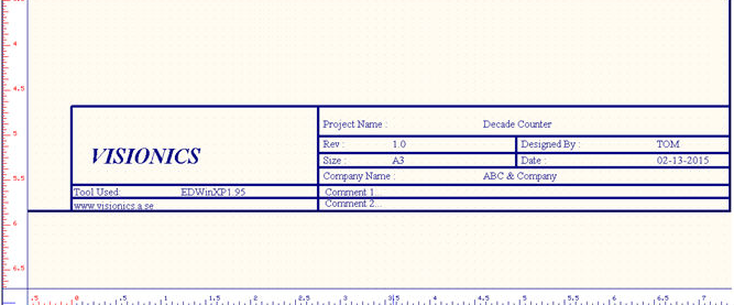
Schematic Editor now contains an auto-generated title block into which user can insert project name, company, paper size etc.
Working
- Select File Menu from EDWinNET Project Explorer.
- Click on 'New Project' option.
- Select File menu from Schematic Editor.
- Select 'Design Title Block' option. A pop-up window will appear as shown below
- After filling the required fields, the title block will be generated as shown below.
 Listing Unconnected Pins
Applies to
- Schematic Editor
There is a new option in Schematic Editor to list unconnected pins. The user can click on pin names that are unconnected and they will be highlighted. The list of unconnected pins can be exported as html report.
Working
- Click on Info menu in Schematic Editor.
- Select 'List of Unconnected pins' option.
- A window containing the list of unconnected pins will be pop up.
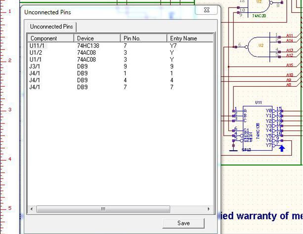
- To save the list of unconnected pins, click on Save button in the tab. The details will be saved as html file as shown below

 Auto-change tool
Applies to
- Schematic Editor
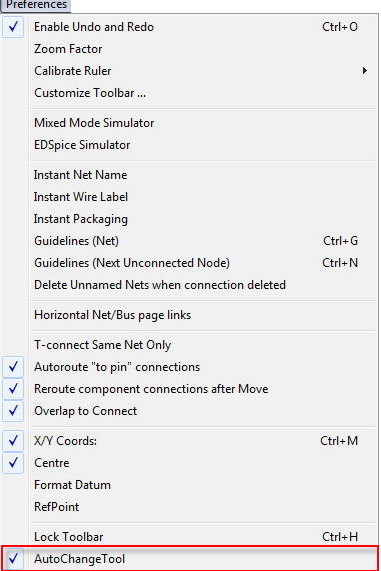
Users can now toggle the “Auto change tool” in Schematic Editor ON/OFF. (By default, the “auto-change” tool is enabled).
Working
- Check whether the Auto Change tool is enabled or not.
- Otherwise, click on Preferences menu and select Auto Change tool.
Tools
Displays a list of menu items that is present in Schematic, Layout and Fabrication
Manager. The menu in this list differ in each editors and when selected allows
entering into main object oriented function.
Tools (Components)
Enters into component editing mode presenting various tools that performs operation
related only to components.
Tools (Connections)
Enters into an editing mode, which presents various tools that performs operation
related only to the connection between components.
Tools (Page Notes)
Enters into an editing mode, which presents various tools that performs operation
related to Notes and Graphics on the Schematic individual Pages.
Tools (Block Edit)
Enters into block editing mode presenting various tools that performs operation
related to objects like components/ wires in block.
Tools (Autoplace)
The tools required to auto place components is displayed automatically on the
workspace when Tools | Autoplace menu is invoked.
Tools (Page Format)
Enters into page editing mode presenting various tools that performs operation
related to editing the default page format.
Tools (Design Notes)
Enters into design notes editing mode presenting various tools that performs
operation related to Design notes.
Tools (Bitmaps)
Enters into bitmap editing mode presenting various tools that performs operation
related to bitmaps.
Tools (Convert truth table to diagram)
Enables conversion of truth table to schematic diagram.
Tools (Convert VHDL Code to diagram)
Enables conversion of VHDL code to schematic diagram.
Tools (Filter Designer)
Enables filter designer to design different types of Active filters by entering
specifications. This will generate Filter circuits in the schematic editor,
which can be used as part of other circuits.
Preferences
Provides a dropdown menu, which may be selected/ deselected to set various features.
These features directly affect the working environment.
Enable undo/ redo:
If this option is unchecked undo and redo options under edit menu remains disabled.
This option provides a faster working environment. Activating/ deactivating
this option in Schematic automatically enable/ disable the operation in Layout
and vice versa.
In the Options window (Project Explorer | System | Options) there is an option for selecting the number of steps for performing the Undo operation. Increase in the number of steps reduces the system speed.
Zoom factor:
Opens an input box that allows specifying the zoom factor. This factor determines
the next zoom level when zoom operation is performed or more appropriately,
the current zoom precision is increased/ decreased by this zoom factor.
Calibrate Ruler:
Allows calibration of the ruler according to user's need. Workspace settings
allow selecting one of four ruler calibration modes.
Operation
Auto: Here the calibration factor will be automatically adjusted to scaling factor (usually in multiples of 2, 5, and 10). By selecting this option the minimum scale value that can be displayed by the ruler adjusts automatically to current precision resulting from zoom up/down operations.
Fixed: By selecting this option ruler will be calibrated in multiples of 10.
Grid: By selecting this option, the ruler will always be scaled as a multiple of the selected grid value. When zoom precision is increased or decreased the grid value may be changed. But the calibration factor will always be the initially selected grid value.
Custom: Selecting this option displays a text box in which calibration factor for scaling the ruler may be entered in the range 1-10. The ruler displayed will always be a multiple of the value given in the text box.
Customize toolbar:
Opens Customize toolbox where users are allowed to select the most commonly
used function tools from Schematic editor and arrange them in custom toolbox.
The purpose of this custom toolbox is to provide direct access to object oriented
function tools, bypassing selection of function tools from different modes (component,
wires). I.e. a collection of function tools of different modes may be customized
to form a Custom toolbar. Skilled users especially prefer this toolbar.
Instant Net Name:
Usually when a wire connection is created, system assigns the first free number
to the nets. But when this option is enabled, system allows to predefine the
net name according to your choice.
Select this menu item from Preferences. Using the Tools | Wires toolbar, start
a wire connection. System instantly pops a window where the name may be specified.
Now every time a new wire/ trace is routed, an input box pops up where the name
for the new net may be entered. If this option is disabled, system automatically
assigns net name (UN1, UN2…) to the newly made connection.
Instant Wire Label:
If this option is enabled, default net label may be obtained at the time of
wire creation. Enable this option by choosing it from Preferences | Instant
Wire Label. On creating a new trace its default name will get tagged to the
cursor. Click anywhere on the workspace to place the label.
Instant Packaging:
Allows to package components as soon as they are loaded into the workspace.
All the constituent groups of the part will be loaded. This is particularly
useful while loading connectors into the Schematic.
Guidelines (Net):
Allows displaying a single ratsnest associated with the selected net while routing
or relocating a wire/ trace.
Select this menu item from Preference and click on any node. The entire nodes associated with that net is displayed as ratsnest. This feature is particularly useful when the layout is prepared first.
Guidelines (Next Unconnected Node):
Allows displaying the next unconnected node associated with the net while routing
or editing.
Select this menu item and click on any of the node. The next nearest node associated with the net is displayed on the page. Take the connection to that node.
Similarly all node of that net may be connected using wire. This feature is particularly useful when the layout is prepared first.
Delete Unnamed Nets When Connection Deleted:
This option when enabled, deletes the whole net when the wire connection is
deleted, provided the net is not named.
Horizontal Net /Bus page links:
This option when enabled, displays net/bus page links horizontally.
T-connect Same Net Only:
Allows T connections to be made only if they are of the same net.
Autoroute "to Pin" connections:
Auto-connector automatically routs last wire segment if the segment is connected
to component pin. When pin-to-pin option is set then every connection is routed.
Auto-connection is disabled when “Option to route only orthogonal connection
segments” is ON or if Preference “Autoroute “to-pin”
connections” is OFF.
Reroute component connections after Move:
The option serves an important purpose of automatic reconnect the nodes of a
component if the component is relocated or swapped.
X/Y Coords:
Allows determining the current cursor position with respect to a given reference
point in terms of the X and Y coordinates/ distance. The values are displayed
in the position toolbar.
This menu item comes under the Preferences menu. When enabled, the X and Y coordinates/
distance values is displayed in the status bar with respect to a given reference
position. The options X/Y Coords and Distance toggles between one another. X/Y
Coords is the default option.
Center:
This menu item comes under the Preferences menu and allows setting the origin
coordinates to the Center. The co-ordinate information displayed in the position
toolbar is with reference to a point on the page. This defines the center of
the page as reference point for all coordinate and dimension information.
Format Datum:
Allows setting the origin coordinates to bottom left corner of the page. The
origin coordinates (0, 0) is now marked at the bottom left corner of the page,
which is set as the reference point.
Refpoint:
Allows setting the position of the origin coordinates on the workspace with
respect to a reference.
Lock Toolbar:
Anchors all the toolbars at the placed location.
Info
The items in this menu provide information about the various objects/items created on the schematic diagram. It allows assessing free symbols, parts, packages, number of nets, etc. The necessary information is displayed in the respective info window.
General
Opens a dialog box where general information regarding the objects placed on the workspace may be obtained. Double clicking the particular object in this dialog highlights the particular object on the workspace. This menu may also be invoked by using shortcut CTRL+F. This dialog may also be used to find particular object on the workspace. There is a slot for Find operation in each tab of this window. In order to find a particular item, select the tab corresponding to the type of object/ item to be searched. Type few characters of the item or select the item from the drop down list. The objects along with corresponding details are viewed in the selected tab. Now click on the particular object/ item on the right side to highlight the selected item/ object on the workspace. Following are the object information’s that can be obtained.
Fig.4. 1
Layout components information: Displays Layout component information window where the layout components used in the current project is listed
Schematic components information: Displays Schematic component information window where the schematic component used in the current project is listed
Parts information: Pops up a window Part Information displaying the list of parts used in the current project (database) and information associated with each part. For EDSpice Simulator, the corresponding window shows the elements currently in use, its status and EDSpice reference ID details.
Packages information: Pops up Package Information window displaying the list of packages used in the current project (database).
Symbols information: Pops up a window Symbol Information displaying the list of symbols used in the current project (database).
Nets Info: Opens a window Net Information that displays information of all nets present in the current project (database).
Buses Info: Opens Bus Information dialog box that provides general information about the buses used in the project (database).
Hierarchy Stack
Opens a window to display information on the current hierarchy and the hierarchy from which the components of the present hierarchy is generated. This menu item may be selected either from General tab window or from Info menu to pop up a window “Hierarchy structure”. Both the dialogs provide details such as name of the current hierarchy used. If the components of the pertaining hierarchy have been generated from other hierarchies, all information regarding the original hierarchies is displayed. The Info window displays only the current hierarchy if the existing hierarchy is not generated from any other hierarchies.
General Settings
Relevant settings of Schematic Editor can be made from the Preferences menu. The following settings may be made in the beginning
1. Enable Undo and Redo – enable this menu to enable Undo and Redo operations. The recommended setting is ON. Turning this OFF will make the system faster.
2. Zoom factor – Pressing the ‘+’ key increases the zoom by a value which is determined by the value of Zoom factor. The default value is 2, i.e. each time the + or – key is pressed, the workspace will be zoomed to double the current value of zoom precision. For smaller changes in magnification on pressing the Zoom buttons, set the value as 1.1.
3. Instant net name – by default when a wire is created, the system allots it a net name UN1, which is by default an Unnamed Net. Enabling this menu will cause an input box to be displayed each time a new net is created so that the user can specify the name of the net. For the purposes of simulation and display of results it is always better to keep meaningful net names. This feature will eliminate the need of renaming most nets.
4. Instant wire label – enabling this option will automatically cause a label to be placed each time a new wire is created. The label will be the name of the net.
5. Guidelines (Next Unconnected Node) – displays a rubber
band connection to the next unconnected node in the selected net. This can be
turned ON while routing.
The above option is relevant only in situations where nets are already assigned.
This is particularly useful for placing and routing projects imported from SPICE
netlists, VHDL etc.
The Grid value can be set to 0.1000”
The Snap value can be set to 0.0500”. For making fine movements, the snap value can be decreased.
It would also be a good idea to enable the following toolbars from the View | Toolbars menu – Function tools, Option tools, Tools, Standard, Sizes, Position and Schematic View
Page Configuration
Before capturing the actual circuit, it is advisable to set the required page size to avoid unnecessary wastage of space. On invoking Schematic Editor page, although a default page outline is provided, user can select pre-defined formats or create own formats.
Features
- Maximum page size available - 4m x 4m.
- Maximum number of circuits /Hierarchies - 99
- Maximum number of pages in a circuit – 99.
- Available page formats – American & European
American formats: A (landscape), B, C, D, E, A (portrait)
European formats: A4 (landscape), A3, A2, A1, A0, A4 (portrait)
By default American format A (landscape) is enabled.
Steps to follow
How
to set page format?
Edit page format
i. Select
Redraw | Page from Standard Toolbar to display the default page within the GUI
window.
i i. To place objects on the page, you may select an object
and simply position wherever required. However, you can exactly position components
by enabling
Ruler from Schematic view toolbar. Ruler gets aligned to the sides of the page
as shown in Fig.4.1 and remains displayed until it is disabled. By default,
ruler is displayed.
iii. Use the function and Option Tools provided to edit the page outline.
How to define page format?
i. Select
Page Format from Tools toolbar as shown in Fig.4.3. The tools in the
ii. Function and Option Toolbar changes simultaneously.
Fig. 4.3
iii. Select
Define Page Function Tool (by default appears selected). The Page format window
appears as shown in Fig.4.4:
Fig 4.4
iv. The page format may be defined by either of the following two ways.
v. Select standard formats (e.g. A4 (landscape)) from the list.
vi. Enter the required height and width in the text box provided and press SIZE OK.
vii. In either of the two options selected, a miniature representation of the page format is displayed in the picture box provided.
viii. Now click on ACCEPT button to reflect the selection.
ix. Select
Redraw | Page from the Tools toolbar to display the default page within the
GUI window.
Schematic Capture
Double click on the task
in the Project Explorer to open Schematic Editor. This tutorial will discuss
the creation of the Schematic Diagram of Half Adder (Refer Fig. 4.5).
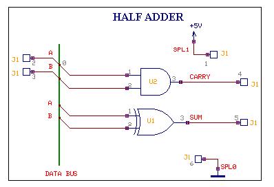
Fig. 4.5
Loading the Components
Before we start loading components on the page, turn ON **Grid
(Grid is the dot raster which when enabled, helps in assessing position and
distance while placing graphical item(s)) by enabling the grid from the dropdown,
in
Standard Toolbar. The value for grid may be selected from the drop down list
as .1000”. Similarly, set Snap value to .0500” for better placement
of the components.
| **Grid is the dot raster which when enabled, helps in assessing position and distance while placing graphical item(s) |
Select
Components from Tools toolbar and right click on the workspace to popup a set
of Component editing tools. By default,
Relocate tool is enabled.
Creating circuit diagram of HALF ADDER:
1. Right click in the workspace and select
Add Components to the Circuit, now click on the option too
Add Components by name from the popup menu. This opens up an input box, enter
7408, (the **Part name of AND gate) and click the ACCEPT button to return to
the workspace with the component attached to your cursor. Click on the workspace
to place it. A copy of the component is still attached to the cursor, so that
the component may be repeated. Since only one instance is required, press ESC.
A-label is attached to the components placed indicating the component name.
In the same way load 7486. Steps 2) 3) and 4) describe another method of loading
components.
Selecting
Add
Components by name tool and specifying the X, Y position together with the angle
of rotation will place a single component at the exact location.
You may also load components from Library Browser which provides options for multiple loading of components, searching for a component, viewing the details of components, etc.
**Part Name is the name by
which a component is available in the market , it is also called ordering
information In EDWinNET components are loaded with their Part
names rather than the symbol names like INV, 2NAND etc |
2. To load 7408 from Library Browser, right click and select
Add
Components to the Circuit and then click on the option tool
Browser to add components tool. Select Parts tab from Library
Browser window that appears. Type 7408 in the Name field. Select 74TTL.PART
from the drop down of Library field and click FIND NOW. The
search results will be listed below.
Drag the item in the list and Drop it on to the Schematic (or right click on the selected items and press Send to / Schematic). Setting all options provided in Library Browser narrows search. For more details on Library Browser, please refer EDWinNET Help. In the same way search for7486. Now the list contains 7408 and 7486. Multi- select both by pressing the SHIFT/CTRL key. Right click, to popup a menu.
Select Send to / Schematic. You will find the Parts placed at X, Y (0, 0) location (by default it is at page datum) in the Schematic. The selected components may also be dragged and dropped to the workspace. If one is not familiar with Part names, select Symbol tab, enter the symbol name, i.e. 2AND, and press Find Now. A list of symbols with the name 2AND appears. Right click on one symbol and select Used by Part / ALL LIBRARIES. A list of parts using the symbol appears; load any on the Schematic using the methods described above.
3. Another method of loading components is by using the Library
Explorer, which can be launched by, right click in the Schematic Editor ->
Add
Components to the Circuit, select the submenu
Explorer to add components. This is similar to Windows Explorer
and it shows all the libraries available in the default Library path. Select
the library, 74TTL.PART and select the parts 7408 and 7486 (press Ctrl key and
select with left mouse click) and load into the workspace by Drag drop / Send
to menu in the right click popup menu.
4. Another method of loading components is by using
the component browser, which can be launched from View->Schematic->Browser
(Refer Fig. 4.6). The required components can be obtained either by using
the Browse option in the window or by Search for the element in the quick
menu. Once the element is found, it can be placed in the workspace using
the Place button in the bin. Hotkeys can also be assigned to element names
by which quick launch of components is possible.
|
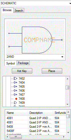 Fig. 4.6 |
5. Half adder needs to make connections to a voltage source, Ground and signal generators for the two inputs. These are external sources (which will not be housed on the PCB) and hence connections to them can be shown with the help of connectors. Take Library Browser to get the pop up window as shown in Fig. 4.7 and type '* 'in the Name field and '*connector*' in the Description field as shown below and press Find Now. The Library Browser will display all the components in the Library with the word connector in its Description (which is entered at the time of Part creation). In the list of parts that appear, select LIST6 since we 6 input output connections.
Fig. 4.7
Load the connector and using 
Add Components to the Circuit and its option tool
Add Components to the Circuit and its option tool Add components by
name (F3).
6. To relocate the component, right click and select tool
Relocate. Position the part where required and click the mouse to place component.
When you relocate a component from a cluster of components, all other components
present may disappear. Clicking
Redraw tool brings the components in view again. The component entries must
be placed on the grid for effective wiring. Proper selection of Grid and Snap
value is a must.
Tip
a) Components may be relocated using bullets. To select (bullet)
a component, press Ctrl key and click on the component. Bullet gets placed on
the component and its function is Relocation. Move the mouse over the bullet.
Now the mouse pointer will change to
move pointer. Click on the bullet and drag to required position.
b) You may use Shift + Z to get a full screen cursor that aligns the symbol on workspace while any operation such as relocation, repeat is performed.
c) Pressing the SHIFT key while relocating/ stretching an item, overrides snap value set allowing the item to move/ stretch smoothly.
***Instead of using Right click
menu for selecting function tools, they may also be activated from their
toolbars which are by default placed on the left of the workspace. These
toolbars are dock able, i.e. they may be relocated and placed anywhere
on the editor window. To lock toolbar position select Preferences / Lock
toolbar (CTRL + H). |
7. With the Function tool
Relocate selected, click on 7408 to select it. The AND gate gets highlighted,
now move the cursor and press left mouse button (or SHIFT + ENTER) to fix the
component at that location. Repeat the same procedure with 7486.
The Parts are placed as shown in Fig. 4.8. The connectors have been placed in
such a way that the end pins, 1 and 6 are devoted for Power/Ground signals.
On packing the pin number to which the entry corresponds to will appear (refer
the picture, all the numbers in grey are the corresponding pin numbers in the
package).
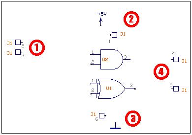
Fig. 4.8
Half adder has six different signals, i.e., A,B,SUM,CARRY,Vcc
and GND. In EDWin XP common terminology for Vcc (+5V) is SPL1 and GND is SPL0.
The printed circuit board requires connections to signal generators for A and
B, these can be made by connectors shown near .location marked 1 in the picture
above,
location marked 2 is for making connections to SPL1, 3 for SPL0 and 4 for output
connections (for signals SUM and CARRY).
Please refer
EDWinNET / Help / Show me How / Schematic Editor / Component editing tools to
view movies illustrating the methods described. Make sure the EDWinNET CDROM
is inserted in the CD drive
Autoplacing the Components
In case of complex circuits you can use the tool
Auto Placer for automatically placing the component in the workspace.
The Auotplacer provide different function as well as option tools for the easy
placement of components . Autoplacer can do the following:
a. It can automatically place all components outside of the page boundaries and sort them according to parts.
b. It allows user to relocate single components and manually place them according to selected placement cell patterns.
c. It allows user to identify other components connected to selected component on the page and manually place them according to selected placement cell patterns.
d. It allows to automatically place components connected to selected one.
e. It allows to automatically place all connected components starting with those connected to selected component.
f. It allows to build groups of components and relocate these groups to desired position on the page.
g. It allows to automatically build new groups of components using the currently present group as template and relocate this newly created group to desired position on the page.
Packing the Components
If the PCB of the circuit has to be designed, then the components
need to be packed. Packaging is nothing but information that the system requires
to identify the Package, associated to Part placed on the Schematic. For example,
symbol **7404 is associated to package DIP14 in layout. Only packed components
are front annotated to layout.
EDWinNET supports three types of packing.
Autopackaging
Select Tools | Component |
Pack/Unpack Component and select
Autopackaging from the option list. An Automatic Packaging window appears
as shown in Fig. 4.9. Click Execute button. The packaging information
appears along with each of the packed components. Automatic packaging assigns
first free number to the last placed component belonging to the same group.
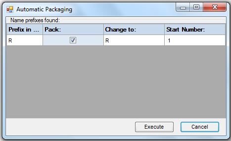
Fig. 4.9
| ***Automatic update of PCB Layout with changes are made in Schematic. Conversely Back annotation refers to automatic update of Schematic with changes made in PCB Layout. **7404 has six INV gates, each
gate is referred to as a group. Parts which have the same kind of groups
are called Homogeneous Parts while Parts like 4000 which have different
groups (3NOR and INV)are called Heterogeneous Parts. |
Instant Packaging
Instant packaging is invoked using the tool under Preferences
menu in Schematic Editor-->Instant Packaging which helps to pack components
as soon as they are loaded to the workspace. All the constituent groups of the
part will be loaded. This is particularly useful while loading connectors into
the Schematic.
Interactive Packaging
Interactive packaging is done using the tool
Pack/ Unpack Component. Right click and select this tool and click on
the component pin that is to be packed. A window “Component Packaging”
pops up (Fig. 4.10). Click ACCEPT button. This method allows individual
packaging of components.
Fig.4.10
Packaging Using Property Window
Packaging can also be done using the property window. This is a form of manual packing, as the user has to select the component (CTRL + Click) to be packed and activate the property window of that component. The steps are as follows for packing component by component:-
1. Select the component by bulleting (CTRL+Click).
2. Right click and select properties to get the Property Sch Component window pops up.
3. In the property window right click on the component and use pack option.
The steps to pack all the components at one instant:-
1. Select Info->General or Ctrl + F
2. Multiple select the components (Schematic component).
3. Right click and select properties to get the Property Sch Component window pops up.
4. In the property window right click on the schematic component and use pack option.
Establishing Connections for the Circuit
Connections between components are established using WIRES and BUSES.
Select
Connections from Tools toolbar to enable a set of tools required for
routing.
Tip:
Adjust zoom precision to view the terminals being wired. Turn ON
grid and snap to help in positioning the wires.
1. Creating the data bus
Select the second Function tool
Create Bus, click on the workspace and drag the cursor and left click
when the bus has the required length, right click and press
End Bus. An input box appears, enter a name for the bus, say Data bus.
The wire connections may now be created in the following way. Before creating
the connections, enable the two menus Preferences / Instant net name and
Preferences /Instant wire label. Right click and select tool
Connect component.
2. Routing the wire connections
a. Enable
Pin to Pin whenever an entry or pin is clicked for making a connection. This ensures that the connection is made to the pin.

Fig. 4.11
An input box appears prompting the user to enter the name of
the net, enter A,n (simply entering A will also suffice). Now select Option
tool
Snap Wire by 90 degree and click on the workspace where the wire
segment has to be bent, now unselect this tool, enable the option tool
Allow T-connections and click on the Bus. An input box will ask which
member of the bus the wire has to be connected to, enter ‘0’. A
text ‘0’ is tagged to the cursor, place it near the wire.

Fig. 4.12
b. Repeat the same process for the second input pin of the AND Gate, in this case give the net name B.
c. Repeat the same process for the first input pin of the XOR Gate. Give the net name A,
d. EDWin gives a message “Connect to existing Net : A”. Press “Yes”.
e. Repeat the same process for the second input pin of the XOR Gate and give the net name B.
f. Enable
Pin to Pin (or press F3) and click on the output pin of the AND
Gate, enter net name CARRY, now enable F2, stretch the wire to a suitable
length and left click. Now terminate the connection by pressing END or F4 key
on the keyboard or click on the tool
End Connection.
3. Routing the wire connection without any visible traces
a. Enable the option tool
Connect without wire from
Connect component function tool.
b. Click on the pin to start connection. The pin is highlighted and the wire extends with the mouse.
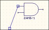
Fig. 4.13
c. Bring the wire end to the required pin and click and then click on
End Connection. The pins as well as the node get highlighted
(Refer Fig. 4.14 & 4.15).
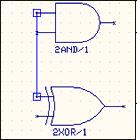
Fig. 4.14
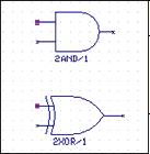
Fig. 4.15
4. Automatic Connection Establishment
Auto routing can take place only if nets exist.
1. Select the option tool
Autoconnect wire to connect a single net or
Autoconnect all wires to connect selected nets.\
2. The Autoconnect dialog box pop up and select the required scheme and click apply.
Tips:
To perform any editing operation on the wire drawn, select the wire
by using Ctrl key. Bullets get placed on the wire. Bullets have function such
as Disconnect wire, Insert Bend point, relocation, etc.
Entering Net labels
To improve the readability of the circuit, use the option tool
Add
/Edit net / Bus member label from the function tool
Edit Connection and click on the wire to be labeled. The net name is tagged
to the cursor. Place the net name at the desired location. Enabling Preferences
/ Instant wire label achieves this but when it comes to bus connections, it
keeps the bus member label instead of the net label. To put the net names in
such cases, use this function tool.
Operations that may be performed on a Net
- Splitting Nets
This function tool may be used to split a net into two parts.
When a net is split then the portion of the net from its starting point to the point of split will retain the same net name whereas the remaining nodes will be assigned to a new net. The new net is automatically assigned a name, which may be changed
- Merging Nets
Existing nets may be merged using this facility. While merging, priority is given to PWR/GND, named and then to unnamed net.
- Deleting Nets
Allows deleting a node or a whole Net.
- Net Properties
Displays the properties of a selected Net, like Net name, status, bus member etc.
How
to merge nets?
i. Select
Edit Connection function tool of connections and the select the option tool
Split
Net.
ii. Click on the wire segment that is to be splitted. The whole net appears selected.
iii. Again, click on it. The selected wire segment thickens to indicate that this wire is to be splitted from the rest of the wires of the same net.
iv. A window pops up where the name is edited.
How
to delete an existing net?
Select
Delete Whole Net or
Delete Single Node from the function tool
Delete Connections/Label to delete net or a node respectively and click
on the nodes. This action deletes the associated wire segment(s) also.
When
a net is deleted, the corresponding trace segments also get deleted. The converse
is not possible i.e. when a trace is deleted the nodes (net) remains unaffected
How
to set net properties?
i. Select
Connection Property.
ii. Click on the node/wire. This pop ups the “Property Nets (Layout)” window.
Entering Page and Design Notes
Select the tool
Page Notes in Tools toolbar to enable a set of tools for creating
page notes.
Fig. 4.16
Right click and enable
Create PN Graphic Item tool and select the tool
Create Text to open a window Add Text as shown in Fig. 4.16. Enter the
required notes and accept it.
The text gets tagged to the cursor. Now place the text at desired position. To edit this text, press Ctrl key and click on the text to select it. Perform the various operations using bullets.
Tip:Page
notes appear only on the current page (e.g. Page No.) of the project whereas
Design notes appear on all the pages (e.g. Project name) of the selected circuit.
To enter the design notes, select Design Notes from Tools toolbar. Enter design
notes using the same tools explained for page notes.
Property window
Purpose
To edit the properties of object(s) after selecting in the Schematic Diagram. Selecting the object(s) by using Ctrl or Shift key, the object(s) or the block is marked with a bullet. Bullets are small filled rectangles attached to certain strategic points on an object.
How
to invoke property window and edit properties of Schematic component?
Select (by bulleting-Ctrl+click) the component first and right click on the workspace. In the pop up menu, choose Properties ? Schematic Component to display the Property window as shown in Fig.4.17.
Fig.4.17
The net name and status can be edited.
In the left pane of the property window, right click on the net name pops up a menu as shown in Fig.4.17.
| Schematic Component | When more than one component is selected (bulleted), all components get listed on the left side of the Property window under Schematic Components. Selecting each component displays its own properties. But, most common properties like (pack, unpack and repack) may be executed by clicking the right mouse button on Schematic Components (present on the left-hand side of the Property window). Similarly, on the right pane vector position, alignment in the X,Y direction and lock/ unlock of the components may be specified. |
| Name | Displays the name of the Schematic symbol tagged to a number (\1). Before packing, this number signifies the number of similar components placed like for e.g.:- 2NAND\1,2NAND\2,2NAND\3 etc.. and after packing, it signifies the group it belongs to. |
| Part | Displays the Part name. We can change the reference of the Part, by entering another Part name in this field. System searches the entire library included in the Search Sequence and displays the part name if available. |
Fig.4.18
| Description | Displays the part description that contains the information of the package and symbols used by this part if available. These information’s are given at the time of part creation. |
| Symbol | Displays the name of the symbol. |
| Symbol description |
Displays the symbol description. These information’s are given at the time of symbol creation. |
| Page | Displays the Page in which the selected symbol is placed. |
| Pos X | Displays the current position (X,Y) of the component with respect to the reference point (by default it is the center of the page). Entering new values may change the position of the component. |
| Pos Y | Displays the current position (X,Y) of the component with respect to the reference point (by default it is the center of the page). Entering new values may change the position of the component. |
| Rotation | The component may be rotated by specifying the angle or by selecting the required angle from the list. |
| Mirror | Checking this option may mirror the component. |
| Locked | Checking this option may lock the component relocation. |
| Subcircuit | Displays the subcircuit that is attached to the symbol. |
| Packaged | This option displays the packaging information of the selected component. |
| Gate | Displays the gate number the symbol belongs to. |
| MM Model Code | If the symbol is assigned a modal code in Mixed mode Simulator or EDSpice code or EDSpice ID then these are displayed in the corresponding field. |
| EDSpice code | If the symbol is assigned a modal code in Mixed mode Simulator or EDSpice code or EDSpice ID then these are displayed in the corresponding field. |
| EDSpice ID | If the symbol is assigned a modal code in Mixed mode Simulator or EDSpice code or EDSpice ID then these are displayed in the corresponding field. |
When more than one component is bulleted, all components get listed on the left side of the Property window under Schematic Components. Selecting each component displays its own properties. But, most common properties like (pack, unpack and repack) may be executed by clicking the right mouse button on Schematic Components (present on the left-hand side of the Property window). Similarly, on the right-hand side, vector position, alignment in the X,Y direction and lock/ unlock of the components may be specified. The information regarding the entry pins of each component may be obtained by clicking on the + icon before each component. This lists all the entries for the each component. Each entry may then be selected to display information such as Pin Number, Pin Attributes, Net Name and the Mixed Mode Sim Name.
How
to invoke property window and edit properties of Schematic component text?
Bullet the object first and right click on the text. In the
pop up menu, choose Properties | Schematic Text to display the Properties window
as shown in Fig.4.19.
Fig.4.19
| Color | Displays the color of the selected text. Color may be selected from the Palette. |
| Rotation | The text may be rotated by specifying the angle or
by selecting the required angle from the list. |
| X Pos | Displays the current position (X, Y) of the component
with respect to the reference point (by default it is the center of the
page). Entering new values may change the position of the component. |
| Y Pos | Displays the current position (X, Y) of the component
with respect to the reference point (by default it is the center of the
page). Entering new values may change the position of the component. |
| Text | Displays the text of the selected item and allows to edit the text. |
| Font size | The size of the text may be selected or specified. |
| Font | The font for the text may be specified. |
| Font width | Allows specifying the font width. |
| Font style | The style whether Bold, Italics, Underline or Strike through may be selected. |
Saving the Project
In order to prevent loss of work, save the project periodically using the following steps.
• On the File menu of Project Explorer, click Save Project or Press Ctrl + S.• The first time Save Project is selected, a dialog pops up prompting to enter the name for the project.
• Type in the name of project as Half_Adder.EPB.
Printing the Schematic Diagram
To print the Schematic diagram, select File/ Print page from the main menu of Schematic Editor. A window pops up with the preview of circuit diagram. Click on ‘Fit to single page’ icon. Click on Print icon to print the page
Miscellaneous
Operations that may be performed after placing a component
How
to change the position of a component?
After placing component on the working area, its position can be altered in one of the following two ways:
• Using Bullets
i. Press Ctrl and click on the component. The component gets selected indicated by a bullet (blue filled square).
ii. Move the mouse over the bullet. The shape of the mouse pointer changes from normal pointer to move.
iii. Click at this point and relocate the component wherever required.
iv. Move the mouse over the bullet and observe the shape of the mouse pointer to change from normal pointer to move.
v. Now relocate the block wherever required
Once
when an object(s) is selected or rather bulleted, you are unable to proceed
with your work, unless ESC key is pressed.
• Using Relocate function
i. Select
Block from Tools.
ii. Select function tool
Relocate Block and click on the workspace.
iii. Block the components and move to the required position.
iv. Click the mouse left button to place the block.
How to Repeat a component?
A component already placed on the workspace may be repeated using the tool
Repeat
Component from Add Component to circuit function tool
i. Select the tool and click on the component. A copy of the component tags to the cursor.
ii. Move to the required location and click to place the component. Another copy remains attached to the cursor unless ESC key is pressed.
.
Step repeat component:
If required, a component may be repeated to the required number
by giving necessary details. This is achieved by using the option tool
Step Repeat Component of this function tool. The number of
components required is entered in the dialog box specifying the number of rows
and columns.
How
to Delete components?
Deletion may be executed in the following two ways.
• Using Bullets
i. Press Ctrl and click on the component. The component is selected indicated by a bullet (blue filled square).
ii. Similarly, keeping the CTRL key pressed select the component one by one.
iii. When the required components are selected, right click on the workspace to pop up a menu.
iv. Select Delete function.
This
method is preferred if you want to delete components in a series placed all
over the workspace where block deletion is infeasible.
• Using Delete function tool
i. Select the function tool
Delete component tool.
ii. Click on the component.
In both the above methods a confirmation box pops up to confirm deletion.
How to delete components enclosed in block?
Objects enclosed in block may be deleted by the following two ways.
• Using Bullets
i. Press Shift and click the left mouse button. A square gets tagged to the cursor.
ii. Drag the square to enclose the required components.
iii. Click the mouse once again to anchor the block. The block gets selected indicated by a bullet (blue filled square) at the anchored point.
iv. Right click on the workspace and select Delete function.
Once
when an object(s) is selected or rather bulleted, you are unable to select tools
and menus, unless ESC key is pressed.
Fig.4.20
• Using Block Delete function tool.
i. Select
Block from Tools.
ii. Select the function toolBlock Delete.
iii. Enable the optionDelete Components in Block and click on the workspace.
iv. Block the components and release the mouse button.
v. In both the above methods, a confirmation box pops up to confirm the delete operation.
Select
the appropriate option tool(s) to delete the desired object(s).
How to Lock/Unlock components?
Tampering of components placed in the working area can be avoided
using
Lock/Unlock Component function tool. Lock/Unlock
by prefix allows locking/unlocking of all the components having the same prefix.
Lock component
i. Select the option tool
Lock by prefix. A window pops up where the name prefix by which components are to be locked is entered.
ii. Type the prefix name and click ACCEPT to lock the components.
Unlock component
i. Select the option tool
Unlock by prefix. A window pops up where the name prefix by which components are to be unlocked is entered.
ii.Type the prefix name and click ACCEPT to unlock the components.
How to change the reference?
The reference of the components loaded can be changed using any one of the following methods.
• Using Library Browser/ Explorer.
i. Open Library Explorer or Browser and click on the component present in the search list.
ii. Press Alt key and drag the component from the Browser or Explorer to the editor and move anywhere over the component which is required to be replaced.
iii. Now, release the mouse.
• Using Bullets
i. Bullet a component (presses Ctrl and click on the component). Right click anywhere on the workspace.
ii. A menu pops up from which select Properties/ Layout Component. Property window pops up where various options are provided for the bulleted component(s) and its entries.
iii. To change the reference, type the required Part name in the Part field. Press enter or click the next row.
iv. The part on the schematic editor is replaced if the component name typed is available in the System Library.
How to find a component?
Following are the two methods to find a component.
• Select Component from Redraw drop-down available in Standard toolbarStandard_Tool_Bar to pop up a window. Type in the Component name and the group number separated by /. For E.g.: U1/1
• This method is much advanced and is obtained by pressing Ctrl+F on the workspace. A window is displayed wherein the information regarding all components are displayed.
Operations that may be performed on a trace after routing
Relocate segment – Use the tool
Relocate segment/ Bend point to relocate the connection segment
/ bend point after routing.
Reroute trace - Use the tool to
Reroute Connection/bus to reroute the existing route path.
Special Operations
Press Ctrl and click on the connection. Now each connection segment of the same net appears bulleted. Each segment is marked with three bullets. |
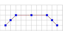 Fig.4.21 |
Each bullet placed on either ends of the connection segment performs move operation whereas the bullet at the center allows inserting a bend point.
Following are the special operations that may be performed when a connection is bulleted.
Right click on the bulleted trace. A menu pops up. |
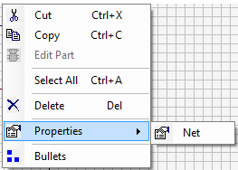 Fig.4.22 |
Menus such as cut, copy, paste, delete, select all does the
function as the name signifies and is similar to any windows program. The property
menu lists a single instant of all objects bulleted on the workspace. To obtain
the properties of trace/ net, click PropertyNet.
Once when an object(s) is bulleted, you will be unable to work with tools and
menus, unless the bullets are removed.
To remove bullets placed on the object press ESC key or keeping the CTRL key pressed, click on the bulleted object again.
Properties of a connection
How to invoke property window and edit properties of trace?
Select (bullet) the object (trace) first and right click on the trace. In the pop up menu, choose Properties/Trace to display the property window as shown in Fig.4.23
Name ................Display the name of the net. This may be changed. Status ...............Display the status of the net whether named unnamed or Pwd/Gnd. In Bus ...............Displays the bus name to which the selected connection (net) is connected.Bus Member ............Displays the Bus Member Number with
which the selected net is identified. |
Fig.4.23 |
Property window is also invoked when you double click on the object (components,
traces, text copper pour item etc.) provided the selected tool on the toolbar
does not perform any function.
How to select text/Design/ Page Notes(s) by marking with bullets?
Press Ctrl and click on the texts/ notes. Now the texts/ notes appears selected with three bullets marked one on each end and at the center as shown in fig.4.24.
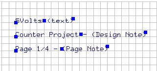
Fig.4.24
E.g. of Text, Design and Page notes
Similarly, keeping CTRL key pressed, click on other text/ notes. All clicked
text/ notes appear selected with three bullets marked on each text/ notes.
Following are the special operation that may be performed when an object is
bulleted.
1. Move the mouse over the bullet present on the left end of the object. The normal mouse pointer changes to MOVE mouse pointer. Click the mouse on this bullet and relocate the text/notes to the required position. Place the text/notes by clicking the left mouse on the workspace. Similarly move the mouse over the bullet at/ on the center/ right end. The mouse pointer will change to CHANGE/ STRETCH mouse pointer. Click to pop up
2. When an object is bulleted, its properties may be accessed in the following way: Right click on the component. A menu pops up as shown in Fig 4.25.
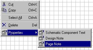
Fig.4.25
How to select Page format by marking with bullets?
Press Ctrl and click on the page format. Now the page format
appears selected with three bullets marked one on each end and at the center
of side.
Following is the special operation that may be performed when an object is bulleted.
Move the mouse over the bullet present on the left end or right end of the page. The normal mouse pointer changes to MOVE mouse pointer. Click the mouse on this bullet and relocate the page outline segment to the required position. Place the segment by clicking the mouse on the workspace. Similarly move the mouse over the bullet at the center. The mouse pointer will change to INSERT mouse pointer. Insert as many as bend points required and click to end adding bend points.
Once when an object(s) is bulleted, you will be unable to use tools and menus,
unless the bullets are removed.
To remove bullets placed on the object press ESC key or keeping the CTRL key pressed, click on the bulleted object again.
How to select Bitmap by marking with bullets?
Press Ctrl and click on the bitmap. Now the bitmap appear selected with a single bullet marked on one side of the bitmap. Move the mouse over the bullet. The mouse pointer changes to MOVE pointer enabling the user to relocate to the desired position. Click the mouse to place the bitmap at the required position.
Once when an object(s) is bulleted, you will be unable to use tools and menus,
unless the bullets are removed.
How to Save and Load a block?
To save block
i. Select
Block from tools.
ii. Select
Save Block function tool
iii. Block the components required to copy
EDWinNET Save Block File window pops up, give a name for the block file to be saved, for example GATES.ESB and click save.
To load block
i. Select
Block from tools.
ii. Select
Load Block function tool
iii. Select stored block file from EDWinNET Select Block File to Load window
that pops up.
