EDWinNET Structure
EDWinNET is an EDA software package for automated design of electronic products.
This integrated tool covers all stages of electronic design process -schematic
capture, PCB layout design, generation of PCB manufacturing and
testing documentation.
EDWinNET is a fully integrated package. Circuit designs can be front and back annotated i.e. a design may be started either from Schematic Editor or PCB Layout and design information is automatically updated. All parts of the designed project are simultaneously accessible by task-oriented modules of the system.
These task oriented modules (see Fig.1.1) are Schematics Editor, PCB Layout Editor, Fabrication Manager and Library Editor
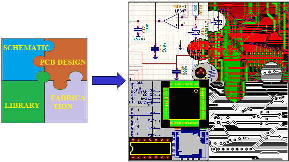
Schematic Editor:Schematic Editor captures the circuit in the form of a schematic diagram. The Schematic Diagram Editor contains a full set of manual and automated tools for placement of circuit elements on the diagram and for routing the connection. Design rules may also set for auto placement and interactive auto routing. Automatic component packaging feature generates pin-out texts on the diagram and prepare the circuit for PCB layout design. Circuits defined in VHDL or in SPICE format netlists may be also imported and converted into schematic diagrams. Due to the integrated structure of EDWin, subsequent design changes in real-time are front annotated to the PCB layout.
PCB Layout Editor:PCB Layout editor includes full set of manual and automated function for designing 32 layered boards. Dedicated full board auto router module is integrated with PCB Layout Editor. Design rules for manual, semi-automatic and automatic routing of traces and component placement can be defined and may be set individually for each project. There are provisions to check design rules violation, clearance errors and missing or incomplete connections of the circuits in this module.
Fabrication Manager:CAM tools grouped in this module allow generating all necessary documents for manufacturing, testing and assembly of printed circuit boards. Fabrication manger also includes reverse engineering tools for reconstructing circuit designs from available manufacturing data in graphical form (artworks in Gerber formats, DXF format drawings etc). RS-274D and RS-274X are supported by EDWin. Gerber ASCII file viewer, an integral part of this module enables to verify artworks before sending them for plotting and manufacturing.
Library Editor: EDWinNET component libraries may be updated, customized or enhanced with the help of Library Editor. Functionality of this module allows definition of graphical representation of components in schematic diagram (Symbol Editor) and on Printed Circuit Board (Package Editor). 2D and 3D views of component packages are created according to IPC, JEDEC and EIA standards.
Integrated Structure of EDWinNET
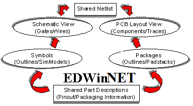
EDWinNET has a totally integrated structure as shown in Fig.1.2. It features seamless integration between all its modules facilitating automatic front and back annotation.
The Schematic and Layout editors make use of the libraries which have shared part descriptions. Part description contains all information about layout view (package) and schematic view (symbols, packaging and pinout) of the component.
When we refer a part, it would extract the physical component assigned at the time of part creation. Some Parts do not contain the symbol information or sometimes the package information. Those parts, containing both symbols and package, will only take part in automatic front annotation to the layout and vice versa.
Components are added to the Schematic diagram from the library and are referred to as Parts; to complete the design we have to establish the connectivity between the components. The connections are created with the support of CONNECTIONS (in Schematic) and TRACES (in Layout) or NETS (in both Schematic and Layout).
The common netlist for schematics and layout is built, through packaging. When a component is packed in schematics, the component pin will get its equivalent pinout information in layout, and are stored as node information. The net consist of nodes and each node has its reference to the components pins both in schematics and layout.
Thus when component in schematics is packed, the layout pin equivalents are retrieved from information stored in part description. Every pin of packed schematics component is checked whether it is a node in some net, if it is a node then the node info is updated. Thus the corresponding package and pinout information's are front annotated to the PCB layout editor and vice versa as shown in Fig 1.3.

Structure of Project Database
All data about electronic design which may consist of several circuits and sub-circuits is stored in a single database, along with PCB layouts. All parts of the project design - schematics, PCB layout and PCB fabrication drawings and documents are simultaneously accessible by task oriented software modules of the system.
An individual project supports circuit with multiple hierarchical levels with multiple pages within a hierarchy. All hierarchies are loaded into memory and stored on disk in a single standard project (.EPB) file. All hierarchies share the local part and libraries. The project allows the user to create up to 99 hierarchies. Each hierarchy may consist of 1 to 99 pages of schematic diagram and a single PCB layout.
There is main hierarchy (MAINHIER) and all further hierarchical circuits that the user creates, are either under this main hierarchy or in equal priority level. The highest level contains a normal circuit, with the other hierarchies being used to capture subcircuits. If required, the designs which are reused can be saved as subcircuits. The circuit can be then referenced as a single component, the subcircuit instance.
Subcircuits can be of two types, hierarchical subcircuits and library subcircuits. Subcircuits may be nested within one another. Subcircuits allow hierarchical construction of designs by grouping the elements of a circuit into a macro. Circuits can be saved as a subcircuit in the subcircuit library and later may be adapted to a symbol.
While simulating the hierarchical subcircuit in Mixed Mode Simulator, the lower hierarchy subcircuit is flattened with upper hierarchy circuit. On other hand in EDSpice Simulator, the library subcircuits (.SBC files) are merged to the spice netlist file. And this entire circuit is simulated.
The fundamentals in designing the PCB are done in Layout Editor. Each hierarchy will have a separate Layout (PCB) associated with it. This means that the entire circuit for a single PCB must be created on the same hierarchy. Any circuit created on any other hierarchy will be created as a separate PCB for that hierarchy.
Integrated Project Database Principles
The integrated structure of the project is explained briefly. You can start with capture of the design in the form of Schematic Diagram. The initial stage will be to place on the schematic, the components, required in the circuit. Assume that one of the components required is IC7400. All the information about this particular component is stored in Part library files
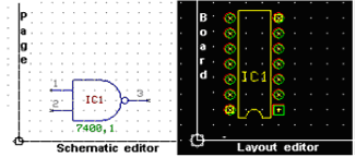
The part library consists of 3 separate but cross-referenced libraries one each for the part descriptions (*.PART), symbols (*.SYMBOL) and packages (*.PACKAGE). The data in the part description stores the information that four gates of 7400 require a 2 input NAND symbol for graphical representation in the diagram (Schematic components), that a 14-pin DIP package is needed to represent this component on the PCB Layout. The part will also contain Pin out information, i.e. information about which pin in Schematic refers to which pin in PCB footprint. These are needed to front annotate circuit components from diagram to PCB Layout - to automatically generate Layout components
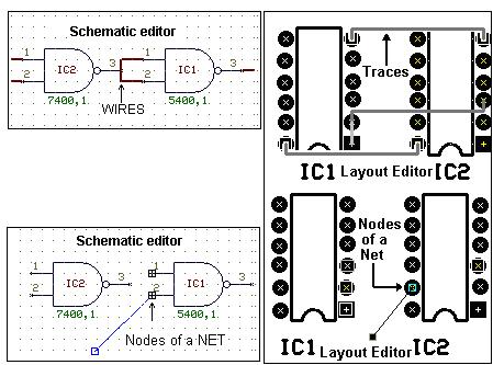
A typical example of components placed in Schematic and Layout editor is shown in Fig 1.5. When the components in the circuit are created, all necessary library elements are loaded from part libraries on disk files and appended to the Project library (local library) within the project. Each new instance of the same type of component requires only a reference to the library elements, i.e. even if there are say 15 NAND gates in the project, the Project Library will contain only one instance. This means that even if several identical components are used in the circuit - they all refer to the same set of library elements in the project (local library).
In addition to the process of creation of components and placing these components on the project (database), to complete the design we have to establish the connectivity between the components. The connections are created with the support of CONNECTIONS (in Schematic) and ROUTE (in Layout) or NETS (in both Schematic and Layout). There are 32 layers available of which 4 layers are reserved for component and solder side silk screens (COMP.PRINT and SOLD.PRINT), component and solder side solder masks (COMP.MASK and SOLD.MASK) and the rest 28 layers as trace layers.
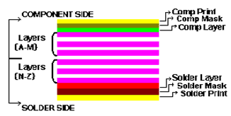
Fig. 1.7 describes logical connections between component entries in the circuit. The net consists of one or more nodes (component entries after connection) and is connected with connections/ traces (physical representation) on Schematic/ PCB Layout. Each Connections/ Trace which may consists of one or more segments is always assigned to a net Therefore operations performed on nets and nodes may result in changes to traces and connections.
In Schematic editor, connections between component entries may also be wired using BUSES. Bus is a group of wires carrying signals. These wires are called Bus Members and should be joined in branches (T-connected) by junction points. Each bus member has a specific number and assigning same bus member number creates merged nets. The net names and bus member numbers may be set under Preference/ Instant Wire label, to appear immediately in the form of movable text labels and may be placed as shown in Fig. 1.8.
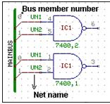
 In
Fig: 1.8, the connection having same bus number belong to same net
Each Trace, which may consist of one or more segments, is always assigned to a net. Nets are considered fully connected if all the nodes in the net have routed connections. All traces, which connect a net, must create an uninterrupted path with branches joined together at component pads or by T-connections to vias or bending points. Trace segments may be placed on any of the trace layers. The board may be checked for errors and rectified to produce an error free board with the Connectivity check and DRC check.
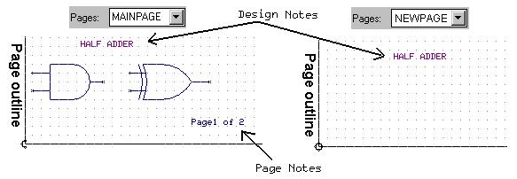
The Design/Page/Board description notes usually consisting of texts and graphics may be used to complete the Schematic diagram and PCB Layout with additional information. The difference between Design and Page notes is that Design notes are common and visible on all pages of the Schematic diagram (For e.g.: Design notes may be used to form the outline of a table, name given to the project which appears on all pages) whereas Page notes are specific to the defined page (for e.g. Page Notes may be used to fill the table with texts containing information regarding the page). See Fig. 1.9 shown for the same project (database). You may notice that design note (HALF ADDER) appear in main page and in new page whereas page notes (Page1 of 2) appears in the defined page.
In the same way as Schematic, the Layout may be furnished with board description notes and dimensions, which may be used during fabrication.

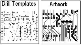
The final step of design process is to generate required design validation outputs and PCB manufacturing documentation. This task is handled by fabrication module. Example for drill data and artwork generated by the fabrication module is shown in Fig. 1.10
Anytime during the work, the whole project (database) may be stored on the hard disk in a single file (extension *.EPB)
Workflow in EDWinNET
Capturing Schematic diagram of the circuit
The user may start to create the integrated design project (database) by either capturing the circuit in the form of a diagram or by designing its PCB Layout. This concept allows building both parts of the circuit design simultaneously. However, the most practical way to design a PCB is to capture the circuit by creating its Schematic diagram first