3 Dimension
Introduction to 3D
Designed electronic circuits (PCB) are usually housed inside cabinets or any intricate structures where spacing between different boards placed has to be dealt with prudently. Working in 3D environment facilitates optical design check. It provides an in-depth analysis of the board density and a realistic view of a designed PCB.
The concept of 3D has been incorporated into Layout Editor and Library Editor especially for package creation. Layout Editor allows only viewing the board in 3D; no editing can be done on the components or traces. But Library Editor allows editing packages and cabinets. Tools have been provided to view the board and package from various directions and from different angles.
Let us have a look at how 3D has been implemented in Layout & Library Editors.
3D in Layout Editor
Layout Editor is provided with two tools namely 3D Board Viewer and 3D Trace Viewer. These tools may be activated from the menu Tools or from Tools toolbar. 3D View Control dialog contains useful tools to control working in 3D environment. These can also be invoked from Layout Viewer.
3D Board Viewer
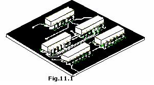
3D Board Viewer gives a real life view of the designed board in various perspectives and directions. It gives idea on how the components are located, whether there is risk of friction between components due to their height and shape, the side on which components are placed, etc. This helps to take any design changes if required. Thus it provides a 3D view of the entire board in any of the X, Y or Z planes from different angles. It also provides the facility to view the board from different directions namely north, south, east, west, etc.Fig.11.1 shows 3D view of a finished board inclined at 45º along X - axis and –65º along Y-axis.
When clicked on
3D board Viewer to get a 3D view of the loaded board a 3D View Control dialog
pops up, which assists in aligning the board in different angles.
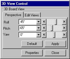
Fig.11.2
Perspective
The controls in this tab allow rotating the board in X, Y and Z planes.
| Roll | To get an angular rotation of the board
along the X plane, select an angle from the drop down list or slide the
corresponding scroll bar. |
| Pitch | To get an angular rotation of the board along the
Y plane, select an angle from the drop down list or slide the corresponding
scroll bar. |
| Yaw | To get an angular rotation of the board along the
Z plane, select an angle from the drop down list or slide the corresponding
scroll bar. |
Click on APPLY button to register the values. Click on DEFAULT button to get the default values.
3D Edit Views
Click on any option to get a corresponding view of the board from that direction.
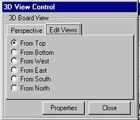
Fig.11.3
Properties
Click on PROPERTIES button to get a dialog as shown in Fig.11.4.
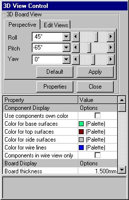
Fig.11.4
Given below is a brief description of each property
| Use components own color | Check this column to allow components use its own color. |
| Color for base surfaces | If Use components own color is not checked, select
color for the base surface from the palette. |
| Color for top surfaces | If Use components own color is not checked, select
color for the top surface from the palette |
| Color for side surfaces | If Use components own color is not checked, select
color for the side surface from the palette. |
| Color for wire lines | Allows selecting color for components outline. |
| Components in wire view only | Check this property to get outline view of components. |
| Board thickness | Allows to specify value for board thickness |
| Display top pads | Toggles on/off the display of top pads. |
| Display bottom pads | Toggles on/off the display of bottom pads. |
| Display holes | Toggles on/off the display of drilling holes |
| Display top side silkscreen | Toggles on/off the display of top side silkscreen (component print layer). |
| Display bottom side silkscreen | Toggles on/off the display of bottom side silkscreen (solder print layer). |
| Display top side traces | Toggles on/off the display of top side (component layer) traces. |
| Display bottom side traces | Toggles on/off the display of bottom side (solder layer) traces. |
| Color for board top side | Choose a color for board’s top surface from the palette. |
| Color for board bottom side | Choose a color for board’s bottom surface from the palette. |
| Color for board edge | Choose a color for board’s edge surface from the palette. |
| Color for board wire lines | Choose a color for board’s outline from the palette. |
| Highlight color for surfaces | Displays color palette to choose a color for surface
of a highlighted component. The component may be highlighted using the
tool Redraw | Component in Standard toolbar. |
| Highlight color for wires | Displays color palette to choose a color for outlines
of a highlighted component. The component may be highlighted using the
tool Redraw | Component in Standard toolbar. |
| Highlight color for lines | Displays color palette to choose a color for print
layers of a highlighted component. The component may be highlighted using
the tool Redraw | Component in Standard toolbar. |
3D Trace Viewer
3D Trace viewer helps to visualize all the physical connections on board. Traces, vias, buried vias, and copper pour elements can be easily visualized. It helps to examine in detail the path taken by traces of each net .Thus it provides a detailed view of all the traces present on the loaded board by aligning the board in various angles. All the traces placed on the component layer may be viewed from top, while the solder layer traces may be viewed from bottom. Viewing the board from any other direction displays the traces present in other layers. It makes the traces present in internal layers (A to Z) visible as shown in Fig.11.5.
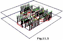
When click
3D Trace Viewer to get a 3D view of the traces present in the loaded circuit.
A 3D View Control dialog pops up, which helps in viewing the trace details from
different angles.

Connectivity Test
The purpose and operation of 3D Trace Viewer Connectivity Test is the same as Connectivity test under function tool Nets.
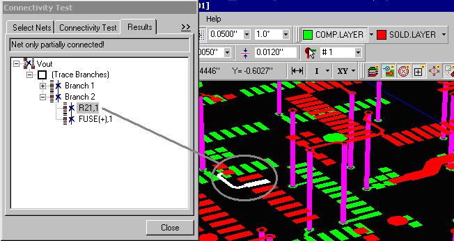
Fig.11.6
However viewing the test results in 3D, gives a deeper insight into the path traversed by the nets thereby helping easy detection and rectification of faulty nets.
3D in Library Editor
In Library Editor, 3D has been bundled with Package Creation. Also a new concept of Board Cabinet has been introduced.
Package Editor
In Package Editor, apart from 3D View Control dialog, a number of function and option tools has been provided to assist the user in editing and orientating the package. A package created in the usual (2D) manner can be converted into 3D using these tools. One can enter the 3D mode from the menu Edit/ 3D Viewer. Package Viewer helps to view the package in 3D.
To begin with, when you open Package Editor in 3D Edit mode, you see a small rectangular box with a round pad on it. This is the same default pad, which appears when a new package is opened in Package Editor. In other words Package Editor gets depicted in 3D mode. Fig.11.7 explains this.
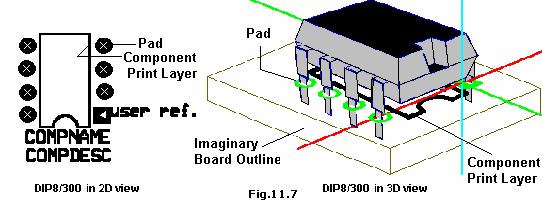
Launch 3D Library Editor
The 3D editor can be launched by selecting the menus - Package Editor | Open Package for Editing - (Enter DIP8/300) / Edit menu / 3D Editor.
The 3D workspace is displayed with three perpendicular axes and a default board containing the outline of the DIP8/300 package as shown in Fig. 11.8.
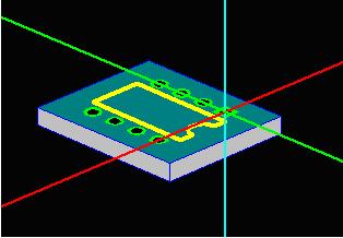
Fig.11.8
The actual view of a DIP8/300 Package is as shown in Fig.11.9.
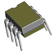
Fig.11.9
A package similar to this figure has to be created using the 3D items. The creation
of the 3D package would have been easy if it doesn’t have a semicircular
notch on the top of the package. There are two ways of doing it. One is to load
a rectangular block and then place a semicircular bar at the location of the
semicircular notch. However to make the 3D view more sophisticated it is possible
to create the package as one composite figure using Polyshape. Since the tutorial
aims to acquaint the user with all kinds of 3D items, the main body is created
as a collection of basic shapes and the pin is created as a polyshape.
The tutorial illustrates how to create the two fundamental parts of the 3D package
1. The main body – consisting of the rectangular bar and the semicircular notch
2. The pin of the package. Once a pin is created it can be duplicated using Repeat Graphic Item option tool.
Main body
3. Select the Function tool Create 3D Graphic Item -> Select the Option tool Create Rectangular Bar.
4. The option tools With Bottom surface, With Top surface and With Side surface(s) may be enabled to get a solid 3D package.
5. Click anywhere in the workspace, a rectangular bar will be placed with the center of its base placed on the intersection of the 3 axes. The rectangular bar will appear highlighted to indicate that the present focus is on it. Relocation and stretching may be carried out here. By default the Function tool Relocate 3D item gets enabled.

Fig.11.10
The rectangular block has to be relocated and stretched to fit in the area 1-2-3-4 as shown in Fig.11.10. The height of the rectangular bar should be set to the height of the body of the DIP8/300 package (this data is available in the datasheet). The height can be set in two ways.
a. Stretch the item to the required height.
b. Enter the height in the Property window of the Rectangular bar.6. Relocate the bar. Relocation of the block may be achieved by placing a contact point. A contact point is by default placed on the intersection of the 3 axes. To move the axes to a desired point press SHIFT and click in the direction where it has to be placed.
7. After moving to the desired location press Finish Relocation(F6)
8. Change the height of the rectangular bar according to the value given in the datasheets.
9. Stretch the bar to fit on the component outline
10. Create the circular patch in the package. Load a semi-cylindrical bar.
11. Elevate the body of the package (both the rectangular bar and the semi-cylindrical bar) by around 15/20 mils (.015”) above the board. This can be done by entering this value in the Properties Window (adjust the Z position).
Creation of pins
So far the creation of the package required only the basic geometric 3D items like rectangular bar, semicircular cylinder etc. Operation on these items is such that their basic shape is always preserved.
For e.g. the item given below when stretched will maintain its aspect ratio, i.e. it will have a proportionate increase in volume since it is a basic 3D item.
Consider a 3D item as shown in Fig 11.11
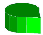
Fig.11.11
This is a composite figure which can be derived from the basic shapes. For e.g.:, a circular cylinder can be loaded on the workspace and it’s angular snap if changed to 30 degree (using it’s Property window) will turn the circular cylinder to a bar with 12 vertices. Now if one edge of this bar is pulled away from the center the composite shape shown in the figure can be obtained.
In order to cater to situations where such figures are needed, Library Editor defines a general term called POLYSHAPE. A polyshape is a 3D item which has been derived from a basic 3D item and whose edges and vertices can be stretched (unlike those of 3D basic items).
The pins of a DIP package are composite figures. Using 3D Library tools, a pin which is shown in Fig.11.12 can be created.
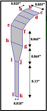
Fig.11.12
This can be derived from a semi-circular strip by stretching its vertices and
edges.
12.1. Load a semi-cylindrical strip on the workspace and move it to a distance away from the other items -> Finish Relocation
2. Set the height of the strip to around 0.055”. This will be length of sides bc / ad etc.
3. Set the number of vertices to 8.
4. Angle B = 90
5. Z Rotation = 90
6. X Rotation = 90
Now the item will look like
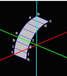
Fig.11.13
13. Once all the settings are made, the semi-cylinder can now be turned into a polyshape so that its edges and vertices can be stretched.
14. Select the Function tool Convert 3D item to Polyshape and click on the semi-cylindrical strip.
15. Creation of face “abcd”
16. Refer the picture of the pin. The length of ‘ab’ is .025”. As a rule of thumb, selection of edges is easier in Perspective View and setting dimensions in 2D views, like From South. Select Stretch item and select the first edge. Now select tab Edit Views in the 3D-view control and select From South. Now move the vertex such that it coincides with the adjacent vertex.
17. After the two coincide, select a Snap value of “ab” i.e. .025”, press Shift key and click in the positive x-axis. Press Finish stretch. The face “abcd” of the pin is formed.
18. Creation of face “efgh”.
19. Select the edge “gh” in Perspective Default View in 3D View Control and then move to the Edit Views -> From South view. First merge the two edges and then select a snap of .065” (the distance separating the edges ef and gh) and click on the negative z axis to complete creation of the face “efgh”.
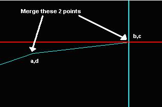
Fig.11.14
20. Creation of face “ghij” and “ijkl” .Select the edge “ij” and merge it with edge “gh” using the same method mentioned in the above steps. Now select a Snap value of 0.065” (distance separating the edges ij and gh) and click in the negative z axis. Repeat the same procedure for the face “ijkl”.
21. As shown in the picture, the length of “ij” is lesser than that of the other edges (0.018”). To set this move to the Perspective Default View in 3D View Control and select the vertex i. Now stretch it along the y axis to a desired position. Press Finish Stretch. Repeat the same procedure with the vertices k and l.
22. Now repeat the pins for the rest of the package and place them in the pad holes in the 3D board of the editor to complete the 3D package of DIP8/300.
Board Cabinet
Printed Circuit Boards are usually housed in complex mechanical structures. These structures can hold large number of such boards. In such situations it becomes necessary to evaluate the spacing between boards, proper utilization of available space, etc.
Board Cabinet Editor helps to create cabinets of various shapes and arrange boards within those cabinets. It assists in editing and orientation of all boards present in the project. It also provides 3D view of all the boards placed, thereby giving a real life appearance of the cabinet as a whole.
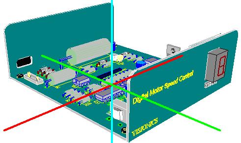
Fig.11.15
Board Cabinet editor window details are mentioned below
Points to remember
Before starting straight away with design in 3D, certain points have to be kept in mind. These include:
• 3D graphic items can be edited only in Library Editor. Layout Editor gives only a real life view of the designed board from various angles and directions.
• You can select pre fabricated 3D elements from 3D elements library while creating 3D packages for components or board cabinets.
• In 2D, mouse cursor can be used to select co-ordinates, by just clicking at that particular point. However in 3D, obtaining the co-ordinates is not as simple as a mouse click since we have to work with co-ordinates placed in 3 planes (X, Y & Z). The three axes act as cursor and to locate a point, each axis has to be moved individually to that point. This is achieved either by clicking on the axes along which the co-ordinates are located or by textually entering the values in 3D View Control dialog.
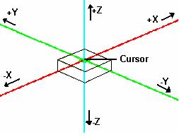
Fig.11.16
• The 3D cursor movement can be controlled either from 3D View Control dialog or by using grid/snap values. For quick displacements of the 3D cursor, press ALT key and CLICK at the desired point on the axis along which the movement has to take place. Using ALT + SHIFT + CLICK moves the cursor to the point and redraws the entire workspace around that point. In addition, the displacement of the cursor and items are also dependent on snap and grid values set. For fine controlled movement, use CTRL + CLICK to get increments with respect to grid value, whereas SHIFT + CLICK gives increments with respect to snap. Precision value determines much finer movements (effective only when snap is OFF). These movements can be easily noticed when working in 3D View Control dialog.
• 3D View Control dialog has all the controls for orientating the board and setting properties of 3D environment. Perspective view helps to select items easily, whereas, Edit Views mode helps in fine editing of the selected item.
• To reduce the time required for redrawing items, enable the display of only the required and most necessary items in the workspace.
• While using 3D cylindrical graphic items, if shape of the item is not of much significance then setting a high value for angular step/ number of vertex in the property dialog, reduces the time required to redraw the items on board.
• Use the property dialog of selected item to carry out swift operations while relocating, stretching, etc.
• Items can be located only at the vertex where the 3 axes meet. Relocation, rotation and stretching of items are all with respect to one of the axis.
Terms to be familiar with:
Polyshape:
Refers to a composite and intricate 3D item derived from any basic 3D graphic item, whose edges and vertices can be stretched.
To obtain a polyshaped item - load any of the basic 3D graphic items, change its angular step using property window (optional), select the function tool Convert 3D item to polyshape & click on the item. The item gets converted and the desired shape can be obtained by stretching the item from its vertices or edges. A 3D graphic item can be converted to polyshape but the reverse is not true.

Fig.11.17
Wire view:
Wire view refers to an outlined view of 3D item. Displaying items in wire view reduces the time required for redrawing the item in workspace.
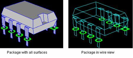
Fig.11.18