Board Analyzers
Types of Analyzers
EDWinXP provides two board analyzers.
Thermal Analyzer
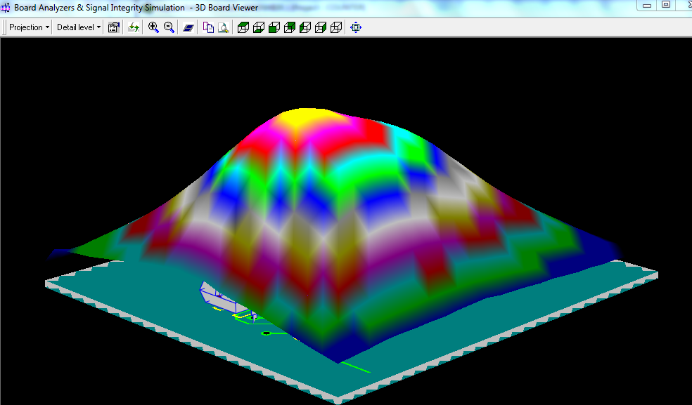
The Thermal Analyzer is intended to be used for analyzing and identifying potential thermal problems on a Printed Circuit Board. It evaluates the Temperature Distribution on a finished PCB, at steady state conditions. From this information, the designer can not only identify potential problems in the design stage itself, but also try out various solutions too - all in an interactive graphical environment. The analysis may be done with the parameters set to appropriate values. The result of the analysis may be displayed using isotherms or color mapping scheme.
Electromagnetic Analyzer
Electromagnetic Analyzer is used to predict the intensity of electromagnetic field generated by the working circuit on the PCB. An electromagnetic field develops when voltage passes through the traces on board. Once the routing of traces is complete, electromagnetic analysis may be performed on the board. The Electromagnetic Analyzer measures the distribution of the Electric Field Intensity on a finished PCB. The isolines show the distribution of the field intensity on the board. Under the electromagnetic analyzer you can perform Signal Integrity Analysis and Field Analysis.
Signal Integrity Analysis
The Signal Integrity Analyzer examines the probable distortion of high-speed signals as they pass through traces on the PCB. The results of the analysis are displayed in the Waveform Viewer. The purpose is to predict how a signal deviates from its ideal (or intended) behavior in a real-world setting.
Field Analyzer
The Field Analyzer is a tool for studying the electromagnetic fields that are created when power and/or signal traces on the board are energized. The results of the analysis may be view as a color graph, isolines, 3D-wire mesh graph, etc. It must be particularly mentioned that, just as with the other two tools, the Field Analyzer does not make any decisions or suggestions about the proper functioning of the design. The Field Analyzer predicts the variations in the selected field, due to electromagnetic properties of physical connections (traces), within a spatial area and time frame specified by the user.
Steps for Thermal Analysis
To understand the thermal analysis, an example project COUNTER.EPB is used.
1. Right click on the task
PCB Layout in the Project Explorer to unfold a list of functions. Clicking on
Board Analyzer in this list opens up this module.
2. From the drop down list of the File menu of Project Explorer, select Open Project and select a project. Load the project COUNTER.EPB from \Job directory.
3. Select the Thermal Analyzer tab.
4. Right click on the workspace and select the tool
Display Parameters. Or select Analysis/ Settings to open the settings window and click the Display Options tab (Refer Fig.9-1). Set the raster to a minimum value (0.025”) and set the Isotherm density to (0.1°C) for better analysis result.
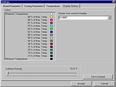
Fig. 9-1
5. Right click and select the tool
Board Parameters (Or select from the Analysis menu). The board parameters are set to the default values by clicking the SET TO DEFAULT button as shown in Fig. 9-2.
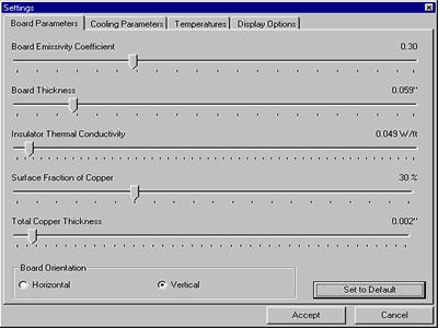
Fig. 9-2
6. After supplying necessary parameters, right click and select the tool
Execute to execute the analysis. The result is displayed in the form of isotherms and color mapping of the board may be viewed by switching on the option View/ Analysis Results/ Colored board.
7. The analysis result is as shown in Fig. 9-3.
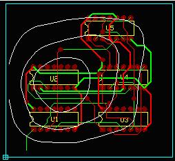
Fig. 9-3.1-Isotherm View
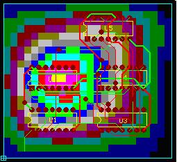
Fig 9-3.2-Color map view
8. From the result it may be easy to identify the most heated component; a heat sink may be used for this. To simulate the heat sink effect, select the tool
Component Parameters and click on the component. A Thermal Parameters window pops up where you may set the cooling parameter for the component. Enter the Thermal Resistance of Heat sink (e.g. 1.2°C/Watt) value and click OK (Refer Fig. 9-4).
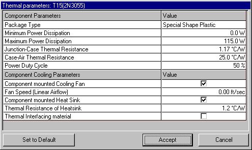
Fig. 9.4
Repeat the same step for all other components and execute the analysis again. You can notice the change in the isotherms after conducting the thermal analysis.
9. Labels may be placed to display the temperature at various points on the board. For this right click and select the tool
Set/ Delete Label and click on the board at required locations. Label gets tagged to the cursor. Now drag the mouse to place the label at proper place.

Steps for Electromagnetic Analysis
To understand the thermal analysis, example project SPICDEMO.EPB is used.
1. Right click on the task
PCB Layout in the Project Explorer to unfold a list of functions. Clicking on
Board Analyzer in this list opens up this module.
2. From the drop down list of the File menu of Project Explorer, select Open Project and select a project. Load the project COUNTER.EPB from \Job directory.
3. Select Electromagnetic Analyzer tab
4. Repeat the same procedure for the other two nets UN2 and UN5 and include these two nets also for analysis. Enter the voltage and frequency value for each net and add to the list.
For example;
UN1 - 5V, 1MHz
UN2 - 5V, 1MHz
UN5 - 5V, 1 KHz5. If you select the SET TO DEFAULT button, the default parameter gets loaded into the text boxes (Refer Fig.9.5).
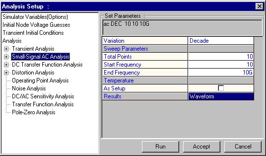
Fig. 9.5
6. View the electrical parameters of the trace from point to point using the VIEW TRACES button (Refer Fig. 9.6).
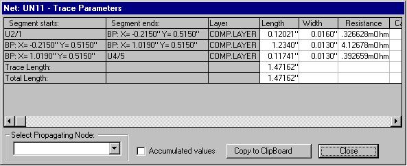
Fig. 9.6
7. After adding these nets you may execute the analysis directly. For this right click and select the tool
Execute Analysis. The result is displayed in the form of isolines. Color mapping on the board and may be viewed by switching on the option Colored board under View/ Analysis Results menu.
8. The analysis result is as shown: The Maximum and minimum field intensity locations are shown in Fig. 9.7.
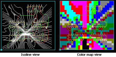
Fig. 9.7
9. Labels may be placed to display the field intensity at various points on the board. For this select the tool
Set/ Delete Isolines and click on the board at required locations. Label gets tagged to the cursor. Now drag the mouse to place the label at proper place.

Steps for Signal Integrity Analysis
Under normal working conditions, signals propagate from some pins of the components in the circuit (technically called Driver Nodes), through the interconnecting traces and into pins on the same or other components (called Receiver Nodes).
Traces have electrical properties like resistance, capacitance and inductance. These parameters are distributed all over the trace and are not concentrated anywhere. The electrical properties of the traces influence the signal as it passes through. For signal frequencies below 1MHz, and trace sizes normally encountered, these influences are so small that they can be safely neglected.
However, above 1MHz, especially close to the GHz range, the electrical parameters of the traces begin to exert significant influence on the signal as it passes through. In this situation, the trace is said to be behaving as a Transmission Line. Sometimes, the effect is so severe that the signal that comes out of the trace is totally different from the one that entered it. As the switching speed of modern digital electronic parts goes well into the MHz ranges, signal integrity problems become more of a concern.
This analysis detects the degree of distortion of the signal from its ideal behavior while it passes through the trace and graphically presents the comparison result with the help of the Waveform Viewer.
To understand the thermal analysis, example project Counter.EPB is used.
Signal Integrity Analyzer is invoked from
within the Electromagnetic Analyzer. Right click on the task
PCB LAYOUT in the Project Explorer to unfold a list of functions. Clicking on
Electromagnetic Analyzer in this list opens up this module.
1. From the drop down list of the File menu of Project Explorer, select Open Project and select a project. Load the project COUNTER.EPB from \Job directory.
2. Right click on the workspace and select the tool
Signal Integrity and click on any of the trace, which is to be analyzed.
3. Now select the net UN6 that connects the nodes of U4/8, U4/12 to U5/3. A window pops up where you may set all the parameters for simulation. To check the integrity of an electromagnetic signal while it passes through this trace, go through the following steps.
4. All nets are displayed in the frame Available Nets. Select UN6 from the list and click
. The segment nodes of the selected net get displayed in the frame Selected Nets. Right click on the node U4/8. The selected node may be set as driver node. From the drop down ‘Function’ select Square Pulse having zero rise and fall times. The electrical properties of the trace will influence the signal as it passes through it and this is shown in the respective columns.

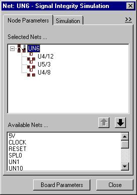
Fig.9.8
5. Set the following parameters.
Max voltage to 5V and
T L->H = 0
T H = 1us
T H-> L = 0
T L = 1us
To set these parameters, click on the respective cell and enter the values and then press the ENTER key.6. The Technology list allows selecting different technologies for both Input and Output pins for the analysis. Select TTL technology from the drop down. The Rout, Lout and Cout parameters are automatically read from the file, Families. EMA that resides in the \SYS directory. The values may be edited by clicking the corresponding box. N/A text denotes that they are not applicable for this family.
7. Next set U4/12 and U5/3 as the Receiver nodes. Set TTL technology to the receiver nodes. Check the check box corresponding to Test Points. The Test points allow to display the output of the selected node in the waveform viewer. If no test point is selected then output waveform alone is displayed on the waveform viewer. Selecting the Driver node and Receiver node automatically selects the interconnecting nodes traces too.

8. The Trace Segment parameters of the driver node may be viewed by clicking on Show Trace Segments (Refer Fig.9-9). Test points may be placed on any of the bend points on the trace segments between the input and output pins by marking the test point check boxes.
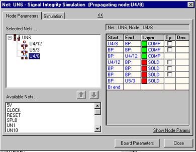
Fig. 9.9
9. To execute simulation, Start time and End time of the simulation as well as the sampling time interval must be specified. This corresponds to the parameters Start time, Time limit and Time step (Refer Fig. 9.10).
10. The CALCULATE button allows to calculate the maximum time limit and will update the text box Time limit. Here the time step is set to 1ns and Time limit to 2us.
11. Various parameters of the board that influence its electromagnetic behavior may also be specified using the button BOARD PARAMETERS. This opens a window that allows to set the parameters for the board such as thickness, electrical permeability and total copper thickness. Click SET TO DEFAULT button to select the default values. All the traced layers to be simulated may be included using the button SET TO TRACE LAYERS USED. In addition to this it also allows to include other layers to make sandwich. To select multi layers use CTRL button and then click the button MAKE SANDWICH. The dielectric in between the successive layers may be edited by clicking the corresponding cell. Click ACCEPT to accept the values
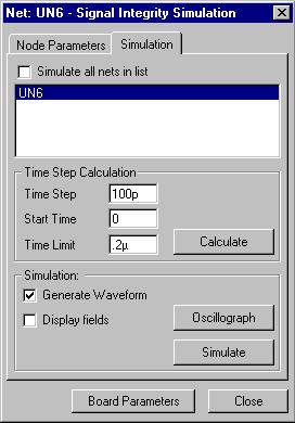
Fig. 9.10
12. The check box ‘Generate Waveform’ should be checked. The result is displayed in the waveform viewer. Checking the option ‘Display Field’ will invoke the Field Analyzer. (See the next section for notes on Field Analyzer). Click the SIMULATE button to process the simulation. The in for one wavelength and a time step of 1ns gives the following result as shown in Fig.9.11.
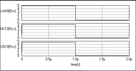
Fig. 9.11
13.Zooming up the particular areas as shown below may identify the distortion levels. You will observe that the signal that comes out of the trace is different from the one that entered it (Refer Fig.9.12).
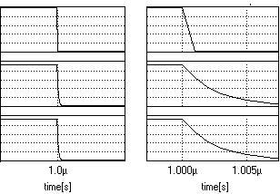
Fig. 9.12


Field Analyzer - Operation
The field analyzer is invoked from the Signal Integrity Simulation window. Follow the steps given for Signal Integrity Simulation to select the trace, receiver nodes, driver nodes, etc. Check the option ‘Display Fields’ in the Signal Integrity Simulation window and click the SIMULATE button to open the Field Analyzer.
From the Field analyzer window, click on the Run Simulation button to begin the Analysis. The maximum and minimum values of the field at each instant of analysis time, within the specified range are displayed. The blue status bar shows the time elapsed and the percentage of total analysis completed.
The simulation may be interrupted (and continued later) at
any desired point by using the
Pause button. This could be very useful to study particular points of interest
within the specified time interval. In order to continue the interrupted analysis,
simply click the
Continue Run button.
Using the
Stop button may stop the simulation. However, doing so will discard the current
simulation and it cannot be continued from that point forwards.
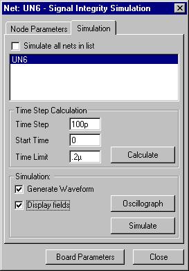
Fig.9.13
Once the analysis starts, information about the field is dynamically presented in two ways:
1. The Field display area will show variation of the selected field type using the graph type specified.
2. Depending on the current choice, the Waveform display area will show eithera. The time variation of the amplitude of the selected field type or
b. It’s spectral content at that moment.
Maximum values of the selected field type within the entire graph area as well as at the probe location are shown in the status bar. These values are updated at every time step specified.
If AutoScaling has been selected, the maximum values displayed as well as the scales of the graphs are automatically updated. On the other hand, if AutoScaling has been turned off, these values are clipped at the values specified. (In other words, values higher than those specified are ignored.)
Using Field Analyzer
The Field Analyzer is started from within the Signal Integrity Analyzer. Before invoking it, the following settings must be done from within the Signal Integrity Analyzer window:
• Select the Net(s), which is to be simulated.
• Select the Driver Node(s) for each Net.
For each Driver Node, specify all required parameters such as Signal Function, Technology, Resistance, Inductance, Capacitance, Voltages, Frequencies etc.
• Select the Receiver Node(s) for each Net.
For each Receiver Node specify Technology, Resistance, Inductance, Capacitance, and Test Points etc.
• Specify the Time Step, Start Time and Time Limit for the Simulation.
• If necessary, specify the required values for Board Parameters.
The Field Analyzer will use these values to perform the simulation.
In order to start the Analyzer, make sure the Display Fields check box is turned on. Clicking on the Simulate button will now bring up the Analyzer window. The Display area will show the following:
1. The board outline along with the layout of the trace selected for analysis, and
2. A waveform display area for showing the Time or Spectral variation of the selected field during Analysis.
A few further settings are necessary within this window before the actual Analysis can be performed. Proceed as follows:
• Set Graph Extent
Size of the square covered by graph
Use the Zoom-Up and Zoom-Down buttons for setting this value. Click Graph Modes
to set the graph extent.
• Specify density of the isolines
Increasing this value will result in a more detailed presentation of results. However, the increased amounts of data generated will result in a slower analysis. Click Graph Parameters to set isoline density.
• Set the Color graph precision raster Size
This value is used to set the precision with which the field values are calculated. Higher values will have greater precision, but take more computing time. Click Graph Parameters to set precision raster of the color graph.
• Set the Color graph display grid Size
This value is used to set the smoothness of the colored graph. Higher values will show smoother variations. Click Graph Parameters to set display grid of color graph.
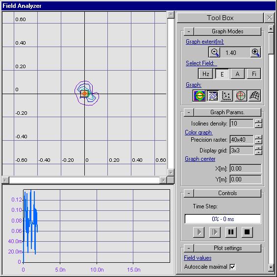
Fig.9.14
• Specify the Time Step value
This value controls the speed with which the analysis is performed. The default value is the same as the value specified in the Signal Integrity Analyzer. Any one of the various multiples of this value, as shown in the drop-down box may be selected. Click Control to set the time step value.
• Relocate the display of the board
The location of the board within the display area can be set using the scroll bars
• Specify the type of field you wish to study and the manner in which it should be graphically displayed.
Any one of four types of field distributions may be selected for analysis. These are
1) Electric field distribution
2) Magnetic field distribution
3) Scalar Magnetic Potential distribution
4) Vector Magnetic Potential distribution
Click Graph Modes to set the type of field distribution.
The fields are obtained by a solution of Maxwell's Equations of Electromagnetism.
These are given below:
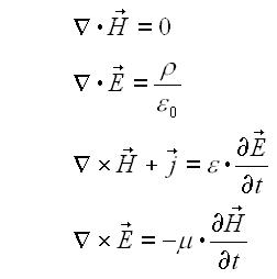
These four equations completely characterize the Electromagnetic field due to the characteristics of signals selected for analysis. Using the parameters that have been specified, these equations are built up and then solved to arrive at a distribution of the field pattern. The equations are iteratively solved over the time period specified so as to obtain the dynamic variation of the field.
Each one of these fields may be viewed in any one of the graph options available. (Depending on your choice of field, some of the Graph options may not be available.)
These are:
| Colored graph | It shows the predicted variation of field
intensity by coloring areas at the same value with the same color. |
| Isoline graph | It uses isolines to represent the field. Areas at the same field intensity fall on the same line. |
| Field direction graph | Directed Lines (Arrows) are used to show the direction
of the field at each point. Applies only to electric field graph |
| Polar coordinates graph | It shows the maximum field intensity in a given direction, with the card placed at the center. |
| 3D wire mesh graph | A 3-dimensional, wire mesh view of the field variation is shown. |
Click Graph Modes to set the type of graph.
• Specify the location of the Probe
The probe is represented by means of a small red circle with
centre lines. By default it is located at the origin of the axes. It can be
positioned at any point in the field display by clicking at that point.
