Fabrication Manager
Introduction to Fabrication Manager
Fabrication is the last stage of the electronic design process. The PCB information is converted into ASCII output files – GERBER (.gbr), NC Drill (.ncd), PCB Assembly Outputs Generic (.pck), IPC-D-355(.355), Bare Board Testing Generic (.bbt) and IPC-D-356A (.356) which is given as input to the machines for creating the hardware.
This chapter explains the fundamentals in generating these ASCII output files. Fabrication Manager also provides a GERBER Viewer to preview the artwork of the output files. The section below provides an overview of the structure and working environment of Fabrication Manager.
Fabrication outputs
The Fig.10.1 shows the outputs generated using Fabrication Manager.
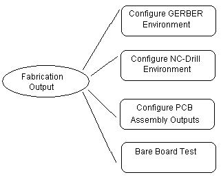
Fig.10.1
The major Fabrication tasks involved in PCB design are as follows.
Fabrication Tasks
• Optional creation of Copper Planes and Copper Pour Areas
• Adding dimensions and notes
• Printing layout documentation drawings
• Extracting NC-drill data to disk files or paper tape
• Editing, dimensioning and printing of drill templates
• Editing and printing of layer artworks
• Generation of artwork data files in GERBER ASCII format
• Preview of artworks of GERBER ASCII files
• Generation of disk files containing generic data for Pick & Place machines
• Generation of disk files containing bill of materials
Before going in detail with Fabrication Manager, refer Fabrication help for the tasks listed above.
Fabrication Manager
The section below provides information on how to invoke Fabrication Manager and describes the general outlook of the working environment.
 How to start
Fabrication Manager?
Click on the task
PCB Layout in the Project Explorer and adopt either of the
following methods.
• Right click on the particular task(here it is
PCB LAYOUT) and select the function (
Fabrication Manager)
• Select the particular function (
Fabrication Manager) from the task list OR from the task toolbar.
The Fabrication Manager window opens with a default board size and gets aligned with the Project Explorer to fit the screen.
General outlook of Fabrication Manager
The Fabrication Manager presented below contains menus and toolbars that control the objects placed on the workspace. Most of the functions are similar to Layout.

File
The File menu item provides the main interface to generate the final outputs. The validation outputs can be generated on printers or laser jet devices. As standard Windows drivers are used by this program, standard Windows commands may be used to get the outputs. However, application oriented interface dialog boxes are provided by the program.
File (Print)
Pops up a window “Preview” that allows previewing the contents on the workspace. It also provides the option to print pages in scales from 10:1 to 1:10 and to set the X & Y offsets.
File (Load Notes)
Opens Select Board Notes to Load window that allows loading notes from another file into the current project. The path and name of the file (*.ebn) of the saved notes are entered in this window, from where it may be extracted.

File (Load Template Notes)
Opens Select Template Notes to Load window, which loads the template notes to the current project. The path and name of the file (*.etn) of the saved notes are entered in this window, from where it may be extracted.

File (Load Graphic Import)
Opens ‘Select Graphic Imports to Load’ that allows loading the graphic data to the current project. The path and name of the file (*.gie) of the saved graphic imports are entered in this window, from where it may be extracted.

File (Save notes)
Pops up a window ‘Save Notes’ to save the notes present in the current project as a file with *.EBN extension. The path and name where the file is to be stored may be set in this window.
File (Save Template Notes)
Pops up a window ‘Save Template Notes’ to save the notes present in the current project as a file with *.ETN extension. The path and name where the file is to be stored may be set in this window.
File (Save Graphic Imports)
Opens a window "Save Graphic Imports" that saves the graphic data. The path and name of the file (*.gie) is entered in this window.

File (Gerber/ Excellon/ DXF/HPGL Viewer)
Opens Fabrication Graphics (Gerber/ Excellon/ DXF/ HPGL) Viewer & Import window that permits the user to import and view the Gerber ASCII files, DXF, HPGL, and Excellon files for viewing and validating purposes before photoplotting.
Special function incorporated in the viewer converts imported data to the categories that may be edited in Fabrication Manager prior to reconstruction of projects from graphics. The viewer also has the capability for automatic distribution of imported data to most suitable category.
File (Copy Screen to Clipboard)
Copies current screen contents to the clipboard.
File (Copy Block to Clipboard)
Copies the contents of the selected block to the clipboard.
File (Exit)
Allows exiting from the currently working module. It also saves the settings made on the workspace for e.g. the view settings, Preference settings etc…
Edit
The Edit menu allows the user to carry out standard edit operations on various objects placed on the workspace. The menu items such as cut, copy, paste, delete, select all and properties are enabled only after selecting (bulleting) objects on the workspace.
| Undo | Reverses the last operation done or deletes the most recently placed object. |
| Redo | Redo reverses the undo action. |
| Cut | Removes the selection of the active page and places it on clipboard. |
| Copy | Copies the selection of the active page and places it on clipboard. |
| Paste | Inserts the contents of the clipboard at the insertion point on the page and replaces any selection. Paste option works only if a cut or copy operation had been done earlier. |
| Delete | Deletes the selected object without putting it on the clipboard. |
| Select All | Selects all texts and graphics in the active window. |
Properties
Displays the properties of the selected (bulleted) objects. Depending on the objects selected, the contents of dropdown list of the properties menu varies. Select this option from the edit menu after bulleting the objects. Properties may also be obtained by right clicking on the selected (bulleted) objects. On right click a window pops up, from which the properties of different objects may be viewed. Some of the properties are mandatory.
Bullet
This feature enables to select (selection by bullets) only a particular group of objects from the selected objects so that the properties of the selected group of objects may be edited. Especially useful when all objects on the workspace is selected.
Layer
A maximum of 32 layers in a multi layered card is supported. These layers are logically divided into two groups of 16 layers each; the first 16 layers are referenced as Component side and the other 16 as Solder side. This menu allows the user to select the various layers of the board. The layers may be selected from the solder side as well as component side.
Tool
Displays a list of menu items and is present in Schematic, Layout and Fabrication Manager. The menu in this list differ in each editors and when selected allows entering into main object oriented function.
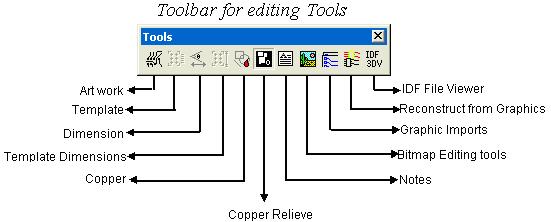
Whenever a tool/ menu is selected, its corresponding function and option toolbars
are displayed, provided these toolbars are made visible using View/ Toolbar.
Tools (Artwork & Pwr/Gnd Planes)
This is merely a print preview of GBR files and various settings in preview can be set. The artwork of a printed circuit board is the actual display of the various copper routes, padstack, pinholes, etc. The design data may be viewed layer by layer as it is got on the photoplotted film or pen plotted artwork. This menu option must be active to view the various layers of the design individually. In order to view any of the layers, use the Layer pull down menu and select the required layer. The artwork for that particular layer may be viewed as it appears on the film.
Creation of Copper Pour Area
On the artworks, Copper Pour Areas are drawn as filled polygons. All traces inside are drawn with airgaps. Pads not belonging to net to which given Copper Pour Area connected is also drawn with airgaps. Pads which are nodes in reference nets and are inside connected Copper Pour Area are drawn as HRF pads as shown in Fig10.4. If they are outside Copper Pour Area, then they are drawn as any other pad.
When the Artwork & Pwr/Gnd Planes menu is invoked “Select layers for preview” opens where the required layers may be selected and click ACCEPT. The artwork as shown in Fig.10.4 appears in the workspace.
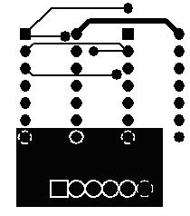
Fig.10.4
Tools - Template [notes]
This menu option is active only when the drill data has been generated using the NC Drill menu. It allows adding manufacturing notes to the template data.
Tools - Dimensions
This menu option provides tools to add dimensions to the layout. For this first define the end points between which the dimension information has to be provided. Contact points are used to define the graphic entity reference points. Dimensioning may be done using the function tools displayed. When this menu option is active the Select Layer option is disabled in the Layer pull down menu since dimensions are usually placed on the Component Print and Solder Print layers. Hence selecting Comp Side and Solder Side items allow to place the notes on Comp. Print and Solder Print layers respectively.
Tools- Template [dimensioning]
This menu option is active only when the drill data has been generated using the NC Drill menu. This template is used as a drawing by the PCB manufacturer to inspect the board drilling, hole size and board dimensions. This menu option provides tools to dimension the template (drill data) created using NC-Drill generation
Tools - Copper
Copper function enables placing of conductive elements on trace layers. Conductive elements may be either of the graphic items - Lines, Arcs, filled and unfilled Circles and Rectangles or a new type of "item" - Copper Pour Areas.
All graphic items are just plain copper. They may or may not be logically connected to nets. Wherever they are placed on the board they may be used to combine copper planes. Each of them may have an airgap defined. They may also be used to draw boundaries of hatched areas, which are in the same category. They are always drawn or photoplotted and any other object placed above them will melt within.
Tools - Copper Relief
This option switches the system to the tools for creating/ editing copper relieve areas. Copper relive areas may be created using graphic items such as lines, rectangles, circles, arcs, polygons etc.
Tools - Notes
This menu option provides tools to add any additional information as well as manufacturing specifications into the layout design. These tools are the same as those used for creating design notes. When this menu option is active the Select Layer option is disabled in the Layer pull down menu since design notes are usually placed on the Component Print and Solder Print layers. Hence selecting Comp Side and Solder Side items allow to place the notes on Comp. Print and Solder Print layers respectively. The following function tool allows editing the layout features.
Tools - Bitmap
This menu option provides tools to add any additional information into the layout design in the form of bitmaps. There is also an option to make these bitmaps visible on all or selected layers of the layout design.
Tools – Graphic Imports
Due to some ambiguity in interpretation of imported graphics or because of necessity to add changes to artworks some elements in categories have to be edited. Editing graphics in Import categories is similar to editing other PCB elements like Notes or Copper. Option is provided to select category for edition. Only element belonging to selected category may be edited at the time but visibility of other categories may be switched ON and OFF.
Editing functions allow to add new elements to category, as well as changing their sizes, locations and (when applicable placement layer). Superfluous elements may be deleted. Graphics elements that were imported to wrong category because of problems with their interpretation in the import phase may be selected and transferred to desired destination.
This menu option provides tools to Import/ Edit the graphic items obtained from the artwork. The tools changes according to the selected Import Graphic Category. The categories may be selected from the Category menu or from the tool bar Layers.
Tools – Reconstruct from graphics
A separate set of tools is provided to execute this task. Tools are arranged in the toolbox in a sequence corresponding to recommended sequence of reconstruction stages. Although the program does not force following this sequence exactly, it doesn’t make much sense to do otherwise. There is not much point in reconstructing traces until components are in desired locations and via holes have been reconstructed. Similarly, reconstruction of net list will not give results without traces.
On the other hand, it is up to the user to decide which objects of Project Database are to be reconstructed. For example, in case of importing PCB outline drawn using AutoCAD, only this part may be reconstructed. The rest of the Project will be designed in usual way.
During reconstruction phase the program displays PCB elements, currently in Project Database. Additionally, the program displays graphics of those categories that form reconstruction template for given type of object. Each time tool for reconstruction of given type of object is selected, the display changes accordingly.
For example, switching to reconstruction of traces causes automatic display category Trace Master. Reconstruction of components uses categories containing pad position as template.
During reconstruction phase “reconstructed” graphic elements are with some exception (pad positions) removed from import categories. It is therefore advisable to save imports prepared for reconstruction in the disk file in case some stage has to be repeated from the scratch. Functions for saving and loading of graphic import categories are available in File menu.
Tools – IDF Import 3D view
Allows importing the selected project contents in IDF standard from any mechanical CAD/CAE system to EDWinXP. To invoke this option, select IDF Import 3D view from Tools menu in Fabrication manager. A 3D Board control dialog box pops up. Here IDB and IDL files are specified and 3D view of the board will be available.
Tools - Bury Vias
Pops up a “confirmation box” to confirm burying the vias. On clicking YES, “Buried Vias Layer Sandwich map” dialog box opens. This dialog box provides information regarding vias present in the loaded project. Click ACCEPT button. The vias will appear only on the intermediate layers enclosed by the layers between which the electrical connectivity is made.
Tools - Unbury Vias
When enabled, it simply unburies the vias. This implies that the vias will now be visible on all layers except on Comp. Print and Solder Print.
Tools - Add Msng Hrf Items
Pads in reference nets may be connected to copper in two different ways. One way is to melt the pad entirely with surrounding copper. The other way is to generate so-called heat relief pads (thermal pads). In this case, the copper is partially relieved around the pin hole leaving through passes which enable connection between pin and copper. The shape and size of such relief pads may be defined by introducing so called Hrf items to the padstacks (Padstack editor). Any of the available graphic items may be used to create the copper relief areas. Normally these items are invisible and the system uses them only to generate Hrf pads of reference nets.
Tools/ Add Msng Hrf Items option maybe used to generate default Hrf items to all those pads where they are found missing.
If the padstack created does not have Hrf item added to it, the Tools/ Add Msng Hrf Items option generates default Hrf items to pads. When this option is selected 'Heat Relief items Auto generation 'window pops up'. If the radio button 'Only in padstacks with missing Hrf items' is selected, then Hrf items will be generated only for those pads where they are found missing. If the radio button 'Regenerate Hrf Items in all padstacks' is selected, then Hrf items will be generated for all pads which belong to the Reference Net irrespective of whether they were already present or not. The Thrupath width and Airgap width for these Hrf pads may be defined in the respective text boxes.

Tools- Add Targets Venting & Thieving areas
Opens Artwork thieving & venting areas, which allows to
set certain PCB Fabrication Aid Items.
For PCB fabrication (especially for multi layer cards) there is a need sometimes
to add certain items to artworks. These items are various graphic patterns which
are used by card manufacturer and normally do not belong to the design itself.
Because of special handling required to include these items in the artworks,
the whole procedure has been added to fabrication (post processing) routines.
Adding fabrication aid items affects printed and photo plotted images of the artworks, CNC-Drill outputs and Drill Templates.
Adding of fabrication aid items is optional. Each item may be selected individually.
Following are the fabrication aid items that can be added to artworks –
1. Layer Alignment Targets |
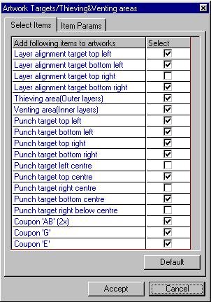 Fig.10.4 |
Layer Alignment Targets (Top/ Bottom Left/ Right)
Specifies whether to add crosswire targets at the specified corner. Bottom left, bottom right and top left corners are selected by default. These targets appear on all layers.
Thieving Area (Outer Layer)
Specifies thieving area to be added to component and solder layers (external layers) and includes empty patches for both types of targets as well as for coupons. Thieving area is used to provide uniform plating for external layers.
Venting Area (Inner Layer)
Specifies venting area to be added to inner layers. Venting area has the same size and contour as thieving area and is plotted as hatched reversed polarity pattern. The function of the hatched pattern is to provide escape channels for entrapped gases when multi layers are pressed together. It includes empty patches for both types of targets as well as for coupons.
Punch Target (Top/ Bottom Left/ Right/ Centre)
Specifies up to nine punch targets in form of crosswire with pad in the center, to be added. Punch targets are for layer registration when the manufacturer uses pin registration technique to align layers. All layers have a hole in the center of the targets and the registration pin helps to align layers when pressed together in multi layer press. The registration hole has drill diameter of 3.2 mm. Punch targets are placed inside thieving and venting areas. Default is six targets – top left, bottom left, top right and bottom right corners as well as top center and bottom center. These targets appear on all layers with exception of Component and Solder Side silk screens.
Coupon AB (2x)
Specifies whether coupons A and B are to be added. User may add two sets of identical coupons along X and Y- axis of the card. They consist of framed pattern of nine (3x3) pads with holes plus surrounding trace pattern. Assigned pad and hole diameter is the smallest found in the design.
Coupon A is used for
(i) CNC drilling
(ii) Back light test for electro less plating
(iii) Solder mask alignment and registration
Coupon B is used for testing
(i) Solder ability
(ii) Thermal stress
(iii) Pull and bond stress
(iv) Rework simulation
(v) PTH integrity
(vi) Etching (setting)
(vii) Miss registration
Coupons are provided for all layers with exception of Component and Solder Side silk screens. In solder and component side mask layers, the pad size is increased by 0.010".
Coupon G
Specifies whether to add Coupon G. It appears as chessboard pattern – square size .050" – and appears on all layers with exception of Component and Solder Side silk screens. In solder and component side mask layers, the square pad size is increased by 0.010".
This coupon is used to check:
(i) Registration of SM with pattern
(ii) Adhesion of SM on copper and epoxy
(iii) Adhesion of plated metals to base metal.
Coupon E
Specifies whether or not to add Coupon E. Coupon E is used for surface insulation resistance. The size (length) and pattern of this coupon depends on number trace layers simultaneously selected for plotting. For each layer a pair of vertically placed pads is provided, starting from top (component side). Pad pairs are repeated side by side for all other layers in the batch. Leads connected to pads move to next pair on each sequential layer.
Preferences
Provides a dropdown menu, which may be selected/ deselected to set various features. These features directly affect the working environment.
Info
The items in this menu provide information about the various objects/items created on the schematic diagram. It allows assessing free symbols, parts, packages, number of nets, etc. The necessary information is displayed in the respective info window.
View
Displays a list of menu items and is present in Schematic, Layout and Fabrication Manager etc. The menu in this list differs in each editor and when selected/ deselected toggles ON/ OFF the display of the corresponding feature on the workspace.
Fabrication
Fabrication (Setup)
Opens Fabrication Data Manager that allows to set the parameters for generating output data to Gerber, NC Drill, PCB Assembly Outputs and Bare Board Test Data Output.
Fabrication (Execute Gerber Template)
Opens window Gerber Output that allows generating a file in Gerber ASCII format containing NC-Drill Template. Select this option and click on execute button to generate the Gerber file for the template. The report file is displayed immediately. The apertures used for the drill template are listed under the Apertures tab.
Export in GenCAM Format
Allows to export the selected project contents to GenCAM format. This is a special format generated which is accepted by photoplotter other than Gerber.
GERBER Output - An Introduction
GERBER is the standard format used as input to photoplotters that generate the design data on films. These films are used as masters for manufacturing the PCB, the physical realization of the schematic data. GERBER format is a vector format for defining various elements of the layout. This format represents all traces as draw and the pads that are part of the component footprint as flashes. The Photoplotter uses this command language.
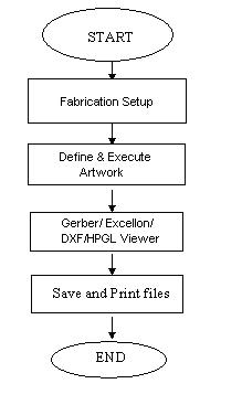
The steps for generating a GERBER output is as shown in Fig.10.6:
{bmc get8_4.bmp}
The layout design has to be defined as an Artwork file to view
the GERBER output format. GERBER output parameters such as Aperture sizes, no.
of copies etc. may then be generated from GERBER setup window. The layers to
be processed may be selected from the tool Artwork
Here the various options such as Mirror image, Via pads etc. may be
toggled Yes/No except for the Copper pour area, which is toggled YES only if
a Copper pour area is created on the board. On clicking this option, a window
pops up showing the net name and an option to toggle generation of Hrf and SMD
pads. Once the Gerber file is generated, its corresponding artwork can be viewed
from Gerber/ Excellon/ DXF/HPGL Viewer
GERBER Output Parameters
Select Fabrication | Setup menu from the Main menu. A window opens from which select the first node select GERBER Photoplotter data and set the necessary data that is required for the photoplotter. Settings include target directory on the disk where the generated outputs such as output units, GERBER format, zero omission, step repeat, scale factor, offset, space between artworks if film is panelized etc are to be stored.
• Output file location
Set the required path where the files are to be generated.
• GERBER Output format
The format of the output may be specified here. RS-274D GERBER format or extended format RS-274X that is, GERBER format with mass parameters with respect to a super set of EIA standards. RS-274X format provides enhancements that handle polygon fill codes, positive/ negative image composting and custom apertures and other features. RS-274X is the default GERBER format.
• Photoplotter options
Photoplotter options such as Interpolation (used to create arcs for the photoplotter), Filled Polygons Supported and Square Flash fill for rectangles for providing information for the photoplotter. Embed Offset & Stepping commands and Mixed Polarity plot is applicable only to RS-274X format. All the above-mentioned options are essentially photoplotter information and cannot be viewed by the user.
Two types of Interpolation may be used when generating GERBER files - Linear interpolation and Circular Interpolation.
| Linear Interpolation | This plots a straight line from the present position
to the X, Y coordinate specified by the data block. Here, steps in degrees
are specified into which the arc is broken as individual segments while
creating the GERBER output. This is always used while generating GERBER
output for lines. |
| Circular interpolation | Instead of line segments and arcs, a quarter of a
circle will be plotted at a time. This eventually reduces the GERBER size.
Even if circular interpolation is enabled, the photoplotter interprets
arc stepping wherever required. |
• Aperture table
If RS-274D is selected, then user may choose the aperture table. If it’s RS-274X, the aperture will be embedded by default.
• Offset and stepping definition
The factors such as offset distance and stepping may be set here.
The required film size is calculated based on the board size multiplied by number of columns and rows plus offsets and spacing between artworks.
Define Layers and Generate GERBER Output
 How to
define layers?
Layers are to be defined first in order to generate the GERBER outputs. Select GERBER Artworks node from the Fabrication setup window. You will find a spreadsheet as shown in Fig.10.6.
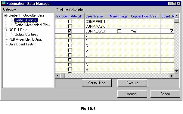

Each layer selected from the list is added to the spreadsheet.

Click EXECUTE button provided in the window or follow the steps below.
 How to
generate GERBER ASCII files?
Click EXECUTE button in the GERBER Output dialog to display the aperture table required for the selected layers.
Here two files will be generated. One is report file, which contains all necessary information for the photoplotter house to properly process user GERBER files. Report file is automatically displayed after finished output. This feature cannot be switched OFF. The other is the *.ALS file which contains list of Apertures used and is optional. Click close to exit. The generated Gerber files maybe viewed/edited with any CAM/Gerber CAM software.
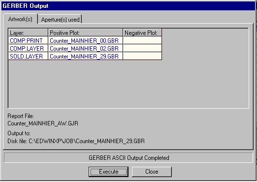
Fig.10.7
Generated files are saved on disk. The file names use the first six letters from the database name. For e.g., if the database is COUNTER.EPB, then the generated files will be as follows COUNTE00.GBR, COUNTE02.GBR, and COUNTE29.GBR. The numbers correspond to the layer numbers starts from COMP.PRINT as 00 and SOLD.PRINT as 31. If the artwork contains Copper pour areas then, files with name suffixes 50+ Layer number (negative) will be generated which acts as the main file (applicable only if the Gerber files are of RS274D format).
This completes the generation of the GERBER data.
Preview the GERBER Data
 How to
preview the GERBER data ?
To preview the GERBER data Select File / Gerber/ Excellon/ DXF/HPGL Viewer and open the .gbr files to be viewed. Different modes of settings may be done using this viewer.
You will observe the selected layer in the display area. For e.g. in figure, GERBER file generated for COMP.LAYER (with Copper Pour Area) of a project is shown in Fig.10.8.
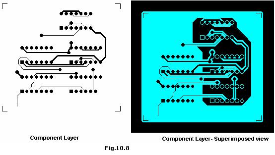
The above procedure must be repeated for all the required layers. Note that once artwork files are created it is possible to switch between preview of different layers by direct selection of one of these files.
Add Notes to GBR Files
Notes may also be generated and viewed in GERBER files generated. These notes form the mechanical details of the PCB layout. The plot may include board outline, dimensions, board description notes, holes and pad.
Select GERBER mechanical plot from Fabrication setup dialog box and set the necessary options.

To display Notes, check Board description notes. When Pad frames option is checked, the layer may also be set. This enables the pad frames of the selected layer on the COMP.PRINT OR SOLD.PRINT. After defining the required settings, click EXECUTE to execute the plot.
Once again click EXECUTE to list the apertures required. By default the created GERBER file has .GBR extension with the first six letters of the file name being the first six letters of the project name and the last two being 90 for component side and 91 for solder side. Here two files will be generated. One is report file, which contains all necessary information for the photoplotter house to properly process user GERBER files. Report file is automatically displayed after finished output. This feature cannot be switched OFF. The other is the *.ALS file which contains list of Apertures used and is optional. For these files the first six letters of the file name correspond to the first six letters of the Project name and the last two will be MK to indicate that it is a mechanical plot file.
Refer Preview the GERBER data in this chapter to preview the resulting plot file.
Introduction to NC Drill
In generating the NC-Drill, the system extracts information about the whole positions, sorts them according to drill size information. The different hole sizes are grouped together and generally sorted to drill in a specific order. This grouping may be done based on sizes, type of drilled hole, like through plated or non-plated, via type like buried or unburied etc. This is generated as a drill tape data. The data may be used directly on any numerically controlled drilling machine. This NC-Drill data is of the EXCELLON format which is the accepted industry standard.
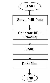
The steps for generating a NC-Drill output is shown in Fig.10.9:
{bmc get8_7.bmp}
Before defining NC-Drill data, it is necessary to set up various parameters. These parameters are briefed in NC-Drill Input parameters.
NC Drill Output Parameters
Select NC-Drill Data from Fabrication data manager dialog box. Depending on the equipment used by the PCB manufacturer some parameters must be set prior to generation of NC drill files.
Parameters include:
Output units: inches or millimeters.
Holes to be included on drill data, component pins and vias are default
Omitted Zeroes: Leading or Trailing. By default it is trailing
Optimization method.

Generate NC-Drill Data
 How to
generate NC-Drill data?
After setting the parameters under the output contents, start
execution of this routine by clicking on
This opens an NC-Drill Output window as shown in Fig.10.10.
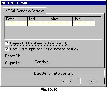
There is an option to generate only the template without generating the drill database and also to check for multiple holes at same location. This may be done by enabling the corresponding check boxes. To output the drill data to template check Prepare Drill Database for template only and click EXECUTE to implement the operation. An additional Report file will be created when the output is taken to the Disk file. This file (*.DJR) should be sent to the manufacturer along with the NC Drill database file. To output the drill data to the disk file (i.e., without selecting the check box Prepare Drill Database for template only), click EXECUTE to pop up a "Select/Define NC Drill File Name" where the path and name of the NC Drill file may be defined to execute the drill generation. By default, the created GERBER file has *.NCD extension with the first six letters of the file name corresponding to the first six letters of the database name and the last two letters corresponding to the layer number in the case of through holes. In the case of buried vias, the file extension is Nxx where "xx" corresponds to the sandwich number. The user is allowed to change only the first six letters of the file name. The text box displays the progress of drill generation. The tool data and the number of holes drilled are also displayed.
Add Dimensions/Notes to Drill Template
 How to
add dimensions to drill template?
Textual and graphic details as well as dimensions may be added to drill template drawing before printout.
To display and add dimensions to drill template select Tools/Template (dimensioning) from the menu bar.
Linear dimensions are generated between positions of two contact points.
Select the
Set Contact Points tool. You may set up to three contact points.
Use the F1 key to set the first contact point at say top left
corner of the board by positioning the cursor at this point and clicking the
left mouse button. Similarly set the second contact point using F2
at say bottom left corner of the board.
Select
Place Dimension tool. You will now see several options to position the dimension
between the preset contact points. Since you have chosen the vertical dimension,
use F1 and click anywhere to the left of the board. You will observe
dimension lines and arrows. Position them alongside the board at a distance
by placing the cursor at that location and click. The text containing calculated
distance appears attached to the cursor. Place the text to the required position.
Dimension text may be rotated during relocation. You can similarly dimension
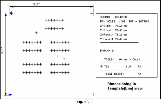
the horizontal side of the board as shown in Fig.10.11.
 How to
add manufacturing notes to drill template?\
Some PCB manufactures require drill template drawing as additional documentation. System creates drill template automatically during NC drill data generation. It contains board outline and symbols for different hole diameters placed at hole coordinates. The legend contains statistics and list of hole diameters with corresponding symbols on the template.
To display and add any necessary manufacturing notes to drill template select Tools/Template (notes) from the menu bar.
The tools are similar to the Design/Page notes in schematic editor.
Introduction to PCB Assembly outputs
When the manufacturing volumes are high and high in component
density, designs like SMD, manual assembly becomes difficult. In such cases,
automatic component insertion technique is required in a specified format to
drive automated machinery to position the components at exact location. As this
data is machine specific, there is a provision for both Generic as well as IPC-D-355
standard format of the output.
{bmc get8_10.bmp}
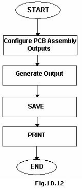
Fig.10.12 shows the steps for generating a Pick & Place output.
 How to
Generate PCB Assembly outputs?
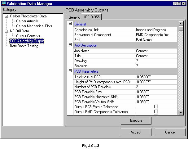
To setup parameters for PCB Assembly outputs choose PCB Assembly output node from Fabrication data manager (Fabrication | Setup).
Introduction to Bare Board Testing outputs
This is a special on board test outputs generated in Generic and IPC-D-356A standard format.
Fig.10.14 shows the steps for generating a BBT outputs
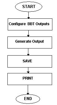
Fig.10.14
 How to Generate Bare Board Test outputs.?
To setup parameters for Bare Board outputs choose Bare Board Testing node from Fabrication data manager (Fabrication | Setup).
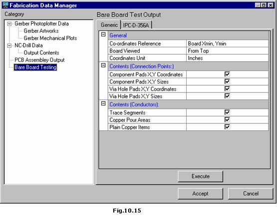
Choose either format and set the required parameters. Click EXECUTE to generate the Bare Board Testing output in either Generic or IPC-D-356A format.
Coordinate reference defines the reference point for generating the pick and place data. Normally, it is in the left-hand bottom corner of the board, the board X min, and Y min. alternatively, it could be the origin of the database.
Contents (Connection Points): Defines the reference point for every component that is to be included into the placement information. The available options are:
Component Pads X, Y Coordinates
Component Pads X, Y Sizes
Via Hole Pads X, Y Coordinates
Via Hole Pads X, Y Sizes
Contents (Conductors): Defines whether the placement data must contain trace segments, copper pour areas, and plain copper items.
Click EXECUTE to generate the pick and place output in either Generic or IPC-D-355.
Coordinate reference defines the reference point for generating
the pick and place data. Normally, it is in the left-hand bottom corner of the
board, the board X min, and Y min. alternatively, it could be the origin of
the database.
Contents (Connection Points): Defines the reference point for every component
that is to be included into the placement information. The available options
are:
Component Pads X, Y Coordinates
Component Pads X, Y Sizes
Via Hole Pads X, Y Coordinates
Via Hole Pads X, Y Sizes
Contents (Conductors): Defines whether the placement data must contain trace segments, copper pour areas, and plain copper items.
Click EXECUTE to generate the pick and place output in either Generic or IPC-D-355.
Graphic Import Editor
Graphic Import Editor makes Reverse engineering possible from GERBER files.
The function of this feature is to import/ reconstruct (reverse engineering process) a PCB from the final outputs generated using any E-CAD/ CAD software (RS 274 format). As of now, *.GBR, *.DXF files can be handled and convert these to intermediary artwork format (This may be done in Fabrication Manager | File | Gerber/ Excellon/ DXF/HPGL Viewer). Finally, using the Reconstruction tool each object is reconstructed individually in order to reconstruct complete or selected parts of Project Database.
Few examples where graphics imports may be used:
a. Complicated PCB outline with or without cutouts have been drawn using AutoCAD. Resulting graphics can be imported and used to reconstruct same PCB outline in the Project.
b. User has old GERBER ASCII files for a PCB that requires changes in the artwork(s) These files can be imported and updated to obtain new corrected set of artworks.
c. User has old GERBER ASCII files for a PCB but needs matching NC Drill data. These files can be imported. Graphic Import Editor has tools that allow reconstruction of drilling data.
d. Reverse engineering: Old GERBER ASCII files may be imported, edited and used as templates to reconstruct complete Project Database.
GenCAM format
Export in GenCAM format - This is a special format generated, other than Gerber, which is accepted by photoplotter.