Library Editor
Library Structure
The library system may be divided into two main parts1. Part Library
This is the main source of information of components and is accessed whenever new components are added to the captured circuit.
2. Simulation Library
Each simulator and analyzer has its special library or libraries. Various elements in these libraries are accessed upon request depending on currently executed type of simulation/ analysis. The library elements in these two main parts are linked together. Typical example is Simulation Function, which is encoded in symbol (part library). Simulation Function instructs simulator, which model (model library), should be used, to simulate circuit element the symbol represents.
Interconnections between different parts of library system are explained in Fig. 3.1.
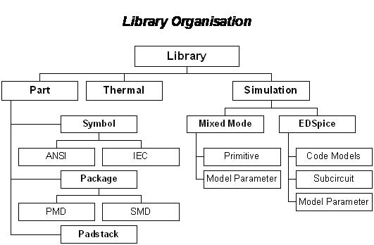
Fig.3.1 Library Organization
Part Library consists of following sections:
Part library files (*.PART) containing parts - part descriptions. Each part is associated with a symbol(s) and one package or with either symbol/ package.
Symbol library files (*.SYMBOL)
Package library files (*.PACKAGE)
Padstack library files (* .PADSTACK)
Simulation Library consists of following sections:
Mixed Mode Simulation Models (* .DLL)
EDSpice Code Models (* .DLL)
EDSpice Subcircuits (* .SBC)
EDSpice Model Parameters library files (* .Sparam)
Mixed Mode Model Parameters library files (*.Mparam)
Part Library
Library files are divided into four categories of disk files - the Part library files, the Symbol library files, the Package library files and Padstack library files.
| |
The PADSTACK LIBRARY contains different types of ready-made padstacks that may be used while creating new packages. |
| The @TOOLS.PACKAGE library file contains symbols for representing different hole diameters on NC-drill Template drawings. The user may edit these symbols if other shapes are required. |
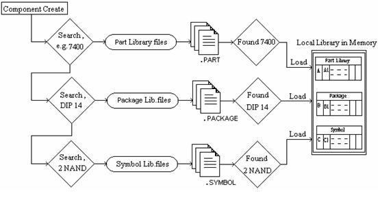
Fig.3.2 illustrates how Part library structure is used in - The Component Create Process.
Fig.3.2 Component Creation ProcessThe libraries *.PART, *.SYMBOL and *.PACKAGE contain the respective parts, symbols and packages. Though the user cannot alter the system library, they can create their own new libraries.
ANSI or IEC Symbols
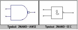
During installation of the EDWinXP, the user has an option to select one of two sets of symbols library - ANSI or IEC Standards.
Fig.3.3 ANSI or IEC SymbolsSymbol representation of 2 input NAND gate – ANSI and IEC standards is shown in Fig.3.3
- The symbols library files (*.SYMBOL) with names starting with "A_" contain symbols created according to ANSI standard (for ex. A_TI.SYMBOL).
- The symbols library files (*.SYMBOL) with names starting with "I_" contain corresponding symbols created according to IEC standard (for ex. I_TI.SYMBOL).
Structure of Part, Symbol, Package and Padstack
Symbols and packages are created independently and saved as *.symbol and *.package. These symbol/packages can then be assigned to a *.part file.
Part Structure
The Part library contains Package and corresponding Symbol attached. In earlier versions of EDWin, (EDWin 16 and EDWin32), Components are loaded on the database as Parts or Symbols or Packages (where components placed only as symbols/ packages are mainly used for simulation/ mounting pins). But now all components created in the Project are referred to as Parts, i.e. symbols/ packages used for simulation purposes/ mounting holes respectively are now created as SPECIAL PARTS where the part may either have symbol or package.
| IEC - International
Electrotechnical Commission |
Even though (unlike EDWin 2000), symbols and packages can be created separately and saved into individual files in EDWinXP, library components can be loaded into a Project only as Parts.
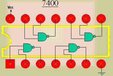
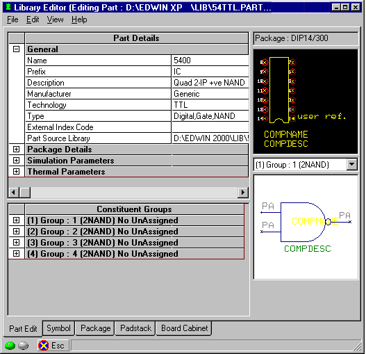
Fig.3.4 Part StructureThe part description contains: Part name e.g. 7400 shown in Fig.3.4 contains 4 groups of NAND gates using the package DIP14.
This is not the actual view but this has been constructed to show how a symbol and package are related to form a Part.
Symbol Structure
The symbol is assigned by - Part Editor | Edit | Add Group or simply by drag and drop of a symbol from Library Explorer to the Library Editor. If it is included in the Search Sequence, the corresponding diagram of the symbol is displayed in the preview.
If there are two or more symbols of the same name, the one which is on top of the Search Sequence gets selected. For e.g.: if a user wishes to use 2NAND of A_CUSTOM.SYMBOL rather than A_DGTAL.SYMBOL, A_CUSTOM.SYMBOL should be placed higher up in the Search Sequence
Fig.3.5 Symbol StructureSymbol name e.g. NAND is shown in Fig.3.5.
If the symbol does not exist or if it has not been included in the Search Sequence, the message “Symbol XXX not found appears. Check whether you have spelt the name correctly. The symbol names are case sensitive”.
Package Structure
The package is assigned by drag and drop from Library Explorer to the Library Editor or by just entering the name in library editor. If it is included in the search sequence, the corresponding diagram of the package is displayed in the preview.
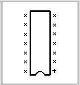
Fig. 3.6 Package Structure
Package name e.g. DIP14/300 is shown in Fig.3.6.
Padstack StructureEvery Component footprint has pins which has physical attributes like diameter (for through hole components) and length/ width (for Surface Mounted Parts). When components are placed on a PCB for connection, these pins must be assigned an area and has to be defined in each of the layers that constitute a PCB. The area occupied by the pins on a PCB is of different shapes and size. Padstack editor serves the purpose of defining the size and shape in each of the layers.
Fig. 3.6 Padstack StructurePadstack name e.g. P_RND_200_H_88 is shown in Fig.3.7.
Creating Library Elements
In this section, we will see how a 2XOR symbol and DIP14/300 package are created and incorporated to form a 7486 part.
Double click on the task
Library in the Project Explorer to launch Library Editor.
This module deals with the creation of the following.
| Creating Symbols |
| Creating Packages |
| Creating Parts |
| Creating 3D Packages |
| Creating Padstacks |
Creating Parts
From the window that opens up on selecting Library Editor, select File | New Part. Enter the name of the part as 7486 and press Enter.
An example is dealt here, with the assumption that package and symbol already exist. Normally, symbol and package has to be created before starting to fill in information for the part. The details to be specified here are:
Under the General column, enter the following information for the new part.
| Name | Name of the part, here it is 7486. |
| Prefix | Part prefix used for packaging, give it as U. |
| Description | Enter a brief description about the component, Quad 2 IP XOR. |
| Manufacturer | Double clicking on this option displays a Select
Manufacture Type dialog box, which lists different manufacture types.
Select the manufacturer name and click ACCEPT to include
this information. |
| Technology | Double clicking on this column displays a Select
Technology Type dialog box from which the standard technologies available
may be selected. |
| Type | Double clicking on this column displays Select Technology
Type dialog box. The component may be specified to be one among the digital,
analog, discrete, or special part. |
| External Index Code | Add External Index Code to the part which helps to
link some external material index in order to fetch additional information
about Bill-of-Material, like prices, manufactures name, name of the part
in local language etc from the EID (External Info Database). |
| Part Source Library | Displays the path of the part. For a new part, displays
[New Part]. |
Under the Package Details column, enter the following information for the new part.
| Package | Package for the part, here DIP14/300, and press Enter |
| Package Type | Double clicking on this displays a Select Package
type dialog box, from which the existing types may be selected |
| Package JEDEC Name | Displays the JEDEC name. |
| Package Source Library | Displays the path of the package. |
Necessary information regarding the Simulation and Thermal parameters may be entered.
To assign symbol for the part, select Edit / Add group and give the Group Name, Symbol and the group before which the symbol has to be inserted (optional) in the pop up text box. Similarly add 4 groups using Add group menu item. Groups may also be added by Drag drop from Library Explorer.
So now we have enough information regarding the Part like its package, symbol. The last section to complete the Part creation is to link between the symbols and the package. For this select Edit/ Edit Pinout to switch to pin out assigning. The menu items under Edit changes accordingly. Easy way of assigning is using Edit/ Auto assign. In the popup text box type 1,1,2,3,1 to complete the assignment for the first two groups similarly type in 3,1,4,3,8 to complete pin assignment for the last two groups.
The Supply Pins GND/ VCC is assigned for pin number 7 and pin number 14.
Creating Symbols
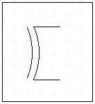
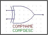
The symbol of 2XOR, shown in the Fig. 3.8, may be created in the following way:
Fig. 3.8 2XOR1. Double click
Library in the Project Explorer to launch the
2. Select the SYMBOL tab in the bottom. The Editor screen appears with a single entry placed on the screen. This entry is located at X, Y location 0, 0 and its entry number is 1 indicated by the “+” sign. An entry is a point at which the connections to a component pin are made. All other entries added later will have an “x” sign. Along with the first entry, the system also places the COMPNAME and COMPDESC text. The COMPNAME refers to the packaged component’s prefix, like U1. The COMPDESC is information about the component like 7486, 74LS86 etc. Zoom down for proper visibility. Turn ON the Grid by enabling the grid from the dropdown
The value for the grid may be selected from the drop down list as .0500”.
3.To create the outline for the 2XOR symbol, click
Create Graphic Item tool and select the tool
Create line.
4. Click the cursor anywhere on the workspace. A highlighted line appears attached to the cursor. This position will denote the starting point of the line. Click the left mouse button to anchor the line. Move the cursor horizontally along the work space unto a point where the required length for the line is obtained. Press the left mouse button to fix the line at the desired position.
5. Place another line, few grids (8) lower but parallel to the first line.
6. Now draw an arc such that it passes through the ends of the two lines. Select the tool
Set Contact Point. Choose
Place Point P1 and click on the point just above the end of the upper horizontal line to mark the starting point of the arc and press the left button to place a point there. Similarly place the second point using the tool
Place Point P2 to mark the end point of the arc.
7. Select
Create Arc from the functional tool
Create graphic item. Click anywhere near the contact point to get a phantom arc tagged to the cursor. After adjusting the size of the arc, click to place it.
8. Adjust the arc, if necessary, by selecting the
Stretch Item function tool and click the
Stretch arc radius tool or press F1 key, to change the radius of the arc. Move the cursor to the inner side of the arc and click. We see the arc’s radius expands and contracts with the movement of the cursor.
Tip: Pressing the SHIFT key while relocating/ stretching an item allows the item to move/ stretch smoothly.
9. Ensure that the arc is of required shape and size. Repeat the same arc using the tool
Repeat Graphic Item and place it as shown in Fig. 3-9.
Fig. 3.9 Placing arc using Repeat Graphic Item10. In the same way draw an arc to define the curved side (near the output pin) of the XOR gate.
11. Place the other arc in the opposite direction.
12. Now select the
Create graphic item tool and select the option tool
Create line and join the entry pin to the periphery of the symbol outline using this line. Since the part of the outline is curved most parts of it do not lie on the grid and hence it will not be easy to stretch the line with the snap settings. The first option is to switch off the Snap (or press SHIFT) and then stretch the line till it reaches the symbol outline. Another (better) option is to change the length of the line using its Property window. To do so, first create a line spanning across two grids (0.1000”). Click in the workspace, keep the mouse over the point of the symbol outline where the line has to intersect it and note the X coordinates (using long cursor is recommended so that the X coordinate selected is on the same horizontal level as the line) and then press ESC. Now invoke the property window by selecting the last Function tool Properties
and the first option tool
Item(s) Properties (F1) and manually enter the coordinates in End X and press enter. Use the
Repeat Graphic Item tool to repeat the line and place it on all the three pins.
13. Place the first/ default entry (+) exactly at the starting point of the first pin of the XOR gate using the
Relocate item tool.
14. We will now place the remaining two entry points Select the
Create graphic item tool and click the
Create entry pin option tool or press F6 key, for creating the entry points. Move the cursor along the workspace to the second input point of the symbol and press the left button. The entry point is placed at the required position and displayed as a small “x” .To view the entry number, switch ON the options View | Symbol | Entry number.
15. Another way of adding an entry is to use the
Repeat Graphic Item tool. Click on an entry, a copy of the entry is tagged to the cursor; place it at the output pin.
Fig. 3.1016. Now the graphical construction of the symbol is over and the Simulation Function of this symbol has to be assigned if the primitive DLL is available.
Refer tutorial on Simulation to learn more about Simulation Functions and primitive DLLs.
Select the option tool
Symbol properties from the function tool
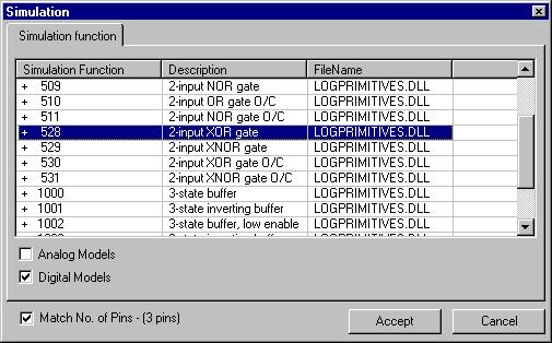
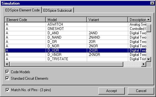
Properties. Triple click (click thrice in quick succession) on the grid cell adjacent to Simulation Function, a dialog box as in Fig. 3.11 listing the available Simulation Functions is displayed. Also, it is easier to get the Simulation Function by selecting the checkboxes Match No. of Pins and Digital Models; a list of all the digital components with the same number of pins appears. Select the one that matches the functionality of the symbol, for the 2XOR symbol, this is +528 and press ACCEPT.
Fig. 3.11 Simulation FunctionIf the symbol is to be used for SPICE simulation, select the grid cell adjacent to EDSpice Element code and click thrice on it in quick succession (triple click) to launch a dialog as in Fig. 3.12, select the model corresponding to 2XOR i.e. D_XOR and press ACCEPT.
Select Symbol type clicking in the grid cell adjacent to it. Browse through the tree view in the sequence Digital | Gate | XOR.
Enter a friendly Symbol description in the grid cell adjacent to it, say 2XOR.
17. Select the
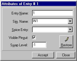
Edit entry attributes tool to give the settings for entries. Click on left top input pin of the symbol created. A dialog box appears containing input text boxes.
a. Entry name - Type IN1 in the text box (any user defined name may be given).
b. Sim Name - Select IN1 from the dropdown list.
c. Spice Entry – Select Input1 from the dropdown list.
d. Visible Pinout – activate check box if the Pinout of the component has to be viewed in the Schematic editor after packaging of the component.
e. Swap level – set to 1.
Fig. 3.12
If the Swap level is set to 1, pins may be exchanged with any other pin. If set to –1, swapping of pins is not possible. For e.g., pins 1 and 2 of the XOR gate can be swapped because both are input pins but the output pin should not be allowed to swap. So we set the swap level for input pin of XOR as 1 and that of the output pin as –1.
Click ACCEPT after completing the settings for the first pin.
Without closing the Edit entry Attribute window click on the second pin and make settings similar to that of first pin and press ACCEPT. Then click on the output pin, make the necessary settings (set Swap Level to -1) press ACCEPT and finally press CLOSE button to return to the workspace.
Fig. 3.1318. After assigning the Simname, we will have to position the COMPNAME and COMPDESC texts. Select the
Relocate function tool. Click on the text and place it at the required position.
19. The display of PIN ATTRIBUTE (denoted by PA) texts alongside the pins may be enabled using View/ Symbol/ PA Text. Select the
Relocate function tool. Click on the PA Text of the first entry and place it near to the pin. Similarly, the PA Texts for all the other pins may be repositioned.
20. Save the symbol to a disk library. If a new library is created, add it to the search sequence. Return to the Part Editor by selecting the Part tab below.
In the same way symbols for NAND, INV etc. may be created.
Tips: To create an arc without defining the contact points, select
Create Arc from the function tool
Create graphic Item and click on the workspace. A phantom arc is attached to the cursor. Position the other end of the arc (not the cursor end) at the point where the arc should start and click. Stretch the cursor to get the required curve and click to complete the arc.
Library Editor creates the symbols automatically using the Symbol Creation Wizard feature. To auto-create the symbols you have to select the option File / New Symbol using Wizard at the start of creating the symbol.
Creating Packages
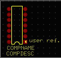
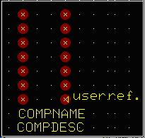
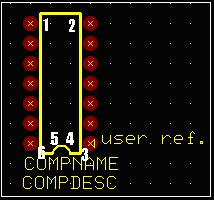
The DIP14/300 (where /300 signifies the pin to pin distance) package, as shown in the Fig.3.14 be created using the following steps.
Fig. 3.141. Double click
Library in the Project Explorer to launch the Library Editor. To start creating a new package, click the tab PACKAGE to open Package Editor.
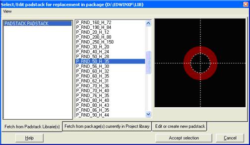
2. Select File / New Package. A single pin with its dimensions appears on the workspace. This entry is located at X, Y location 0, 0 and its first pin. Each pin of the physical component has a specific size. To assign this size information, we will have to specify a padstack for each pin. Select the Function tool Change Padstack
and its option tool Select Padstack
and click on the workspace to pop up a window as shown in Fig 3.15.
Fig. 3.153. Choose an existing padstack P_RND_50_H_35 and click Accept selection. Now draw a block around the padstack to change to the selected one.
Tip: We may view the actual size of the pin by choosing View | Package | True Size.
4. Select the
Repeat Graphic Item function tool to repeat the pads. Select
Step Repeat item option tool to repeat it in steps. Click on the center of PAD/ PIN already positioned. The Step Repeat menu will appear and it prompts for the inputs viz. steps, dx, dy. Since DIP14/300 contains 14 pins placed equally on either side, we enter the following information 6, 0, 0.1. Click OK to place pads on one side vertically upwards with the difference of 0.1 inches.
5. Now we will start the second row of pads for the IC. UnselectStep Repeat Item, click on the 1st pad and then move the cursor by the inter-pad distance (for DIP14/300 it is 0.3000”) and place the 8th pad.
6. Now we may repeat the above step to create another 6 pads of the DIP14. Click on the eighth padstack. The dialog box appears. Type 6, 0, -0.1. We will find another set of 6 pins have been created.
7. All 14 pins of the IC are placed. We have to create an outline for the part. The outline should be on the Comp. Print layer in board design. Hence this rectangle must be created on this layer. To select the layer on which to create drawing items, go to Layer | Select Layer | Comp. print or simply select COMP.PRINT from Layers toolbar (Toolbar can be displayed by View | Toolbars | Layers). This will set the layer as COMP.PRINT for creation of graphic elements.
Fig. 3.168. Select
Create Graphic Item tool and then
Create line option tool to create a rectangle border around the pads. Now turn ON the grid, and set the grid and snap size. Click on the workspace. A small line will appear at the cursor. Move the cursor to the point where the graphic should start and press the left mouse button. As we move the cursor, the line is stretched, left click on completing one side. Refer picture below and create the lines 1-2, 2-3, 3-4, 5-6 and 6-1. As per the general convention usually a small curve is present in the outline to identify the starting point of pin numbering. Place contact points on 4 and 5 and create an arc on the outline using the tool
Create Arc as shown in Fig.3.17.
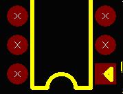
Fig. 3-179. The IC’s first pin is generally a square pin. This is to help identification for assembly. We will then have to change the shape of pad for pin 1. Change the padstack assigned to this pin from P_RND_50_H_35 to P_SQR_62_H_35. For this, we will first have to select the
Change Padstack. Press F1 key and click on the padstack (First one) which is to be changed. The Select Padstack window pops up. Select the tab Padstack. Choose the required padstack, here it is P_SQR_62_H_35. Click SELECT to return to the workspace with the padstack replaced. Pin 1 is now a square pin.
Fig. 3.1810. Enable the
Relocate function tool and click on the COMP NAME text. We see that the text gets tagged to the cursor. Drag and position it near the top of the symbol at the left top corner. This defines the position for the component designator in the layout.
11. Select File menu | Save Package and save it to a disk library.
Creating Padstacks
Now we will see how to create a padstack RND_PAD, as shown in the figure below, using the following steps
Fig. 3.191. Double click
Library in the Project Explorer to launch the Library Editor. Click the tab PADSTACK to open padstack editing mode.
You may create the padstack using two ways. Either by entering the padstack details using the wizard or by manually editing the default padstack in the workspace.
Creating a new padstack automatically
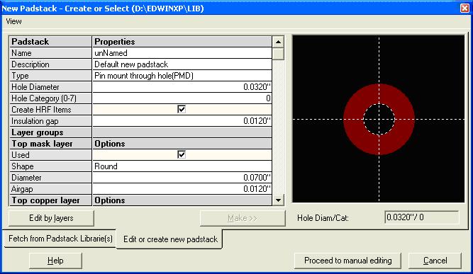
1. Select File | New Padstack using Wizard. to pop up window as shown in Fig.3.20.
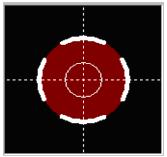
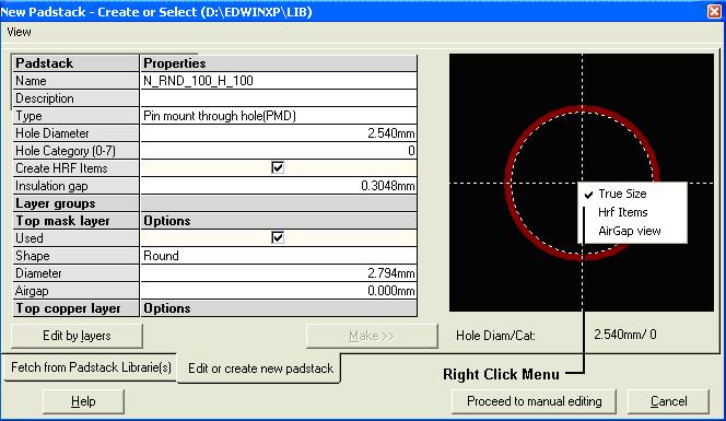
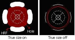
Fig. 3.202. In the window, a miniature representation of the padstack is shown in the preview. Right click on the preview for options to view True size, Hrf items and Airgap view. From the Fetch from Padstack Library(s) tab, select the padstack “N_RND_100_H_100”. Now on moving to the Edit or Create New Padstack tab, the padstack details of “N_RND_100_H_100” appears.
Fig. 3.21The minimum information required to create a New Padstack is given in the Fig.3.21. The user may edit the values
Name = N_RND_100_H_100 and press the <enter> key.
Create HRF items = select the checkbox
Airgap = 0.0120"
Hole Category = 0
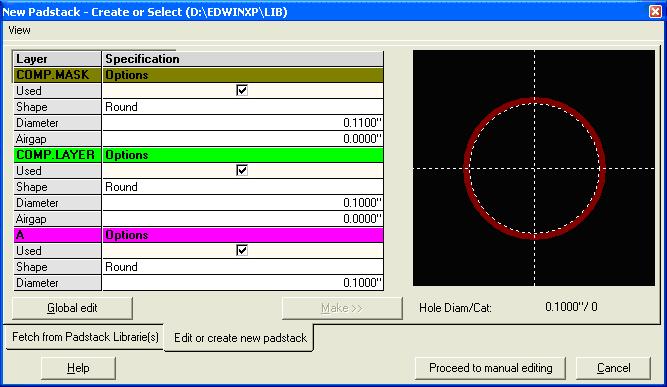
Hole diameter = 0.1000"On clicking the Edit by Layers button, the pad details of different layers (Shape, diameter, Airgap and the option of selecting the layers to be used) appears.
Global Editing of layers is also allowed.
Fig. 3.22Finally click the button Make to create the new padstack. Now the edited changes are visible in the Preview in the right pane. Click on Proceed to manual editing to effect the changes and exit.
This completes the Padstack creation using wizard. The edited padstack appears in the Padstack editor and further edition can be done using the tools available.
File | Save Padstack | Padstack name.Create the padstack manually
1. From the Library Editor /Padstack tab. (The editor opens with a default new Padstack creating and editing window).
2. Click on proceed to manual editing button. The editor opens with a new Padstack.
3. Set the hole diameter using the tool
Properties/
Padstack Properties. Enter the hole diameter as 0.035” and hole category as 0. On clicking the ACCEPT button you may see that the hole is placed on the workspace, indicated by dotted lines.
Fig. 3.23
Tip: Zoom up or zoom down to get a clear view of the hole as shown in the figure above.
4. Now you have to create the pad for each layer.
5. Select the
Create Graphic Item function tool and select the
Create Circle option tool to create a round padstack.
6. Click the mouse on the workspace. A small circle gets placed on the workspace. To obtain the required size, you have to stretch the circle using the
Stretch Item function tool.
Tips: Pressing the SHIFT key while stretching an item allows to stretch the item smoothly to any size. Switch off View/ True size while selecting an item for stretching or relocating.
Using
Place Contact Points function tool; you may easily create the circle. Place two contact points P1 and P2 as the start and end points of the diameter of the circle. Then select the
Create Circle tool and click the mouse. You will see the circle being created automatically enclosing the placed contact points.
Now you have created a single layer pad.
Fig. 3.24If you want to create the pad for all layers, you have to repeat the graphic item 32 times using the
Repeat tool. Press the ESC button or the ESC key to stop the process of repeating items. Then change the layers for each item using the tool
Properties/
Item Properties and assign each graphic item to different layers.
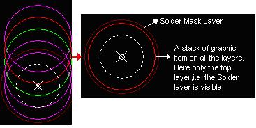
Finally keep these items one above the other such that the hole comes in the center of the stack to get a single padstack. Select the
Relocate tool to place the circles together.
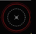
Usually the diameter of the graphic item for the Solder mask layer and Component mask layer is kept slightly greater than that for the inner layers. So, in the figure above you can notice that the outer circle (Solder Mask) is bigger than the stacked circles.
Tip: To view any layer in the padstack, select View | Active Layers. A window pops up. Toggle the status of the layer you want to view as YES and keep the status of all other layers as NO. Click ACCEPT to return to the workspace with the selected layer displayed.
7. The HRF item may be created using the tool
Create Graphic Item/
Create Hrf Pad along with
Create Arc tool enabled. Define the contact points with the tool
Set Contact Point. Then select
Create Graphic Item with both the tool
Create Hrf Pad and
Create Arc tool enabled. Draw arcs to surround the padstack as shown in fig. 3.24.
Fig. 3.258. Save the padstack by selecting File | Save Padstack from the Padstack Editor window. To edit an already existing padstack, select the padstack from Library Explorer and right click to pop up a menu. Select Edit Padstack for editing.
Library Explorer
The function of the tool Library Explorer is to provide the user with the list of available libraries. All library components in each library are displayed irrespective of the libraries added in the search sequence. This is especially useful for copying and moving components from one library to another. Apart from this, user may also place components (included in the search sequence) on the schematic/ layout. You can open the library that contains the file you want to move or copy, and then drag it to the library you want to put it in, provided they belong to the same category.
Similarly, operations performed in the search list of library browser are applicable here. New libraries may be created with much ease.
All the libraries including system and custom libraries will be displayed in the explorer irrespective of whether the custom libraries have been included in the search sequence.
Starting Library Explorer
1. Click on the option tool to
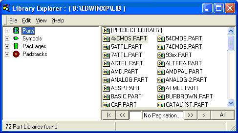
open Library Explorer as shown in Fig.3.26.
2. Click on any directory to open up folders. (For e.g.: Part).
3. Click on any of the libraries to display list of library elements present in the selected library.
4. Select the component(s) from the list and drag & drop into the layout editor or Send to/ Layout.
Another copy of the drag and dropped component remains tagged to the cursor unless ESC key is pressed.
Fig.3.26. Library ExplorerPart Library
Displays a list of part libraries in the Library Explorer window and is mainly used to create new Part libraries, to copy/ move components to different part libraries. Also the symbol and package that comprises the selected part may be viewed using the viewers. Another major use of this explorer is that user may place components on the editors from here.
Symbol Library
Displays a list of symbol libraries in the Library Explorer window and is mainly used to create new Symbol libraries, to copy/ move components to different symbol libraries. Also the symbol may be viewed using the Symbol Viewer.
Package Library
Displays a list of package libraries in the Library Explorer window and is mainly used to create new Package libraries, to copy/ move components to different package libraries. Also the package may be viewed using the Package Viewer.
Padstack Library
Displays a list of padstack libraries in the Library Explorer window and is mainly used to create new Padstack libraries, to copy/ move components to different padstack libraries. Also the package may be viewed using the Padstack Viewer.
Drag & Drop feature
- Select the component(s) displayed (using SHIFT or CTRL key).
- Click the left mouse button.
- Drag the mouse to Schematic or Layout editor.
- Release the mouse. The component(s) tags to the cursor with the
Relocate function tool enabled.
- Click the mouse left button to anchor the component(s) at the correct position.
Send to feature
1. Select the component(s) in the explorer.
2. Click the right mouse button. A menu pops up where select Send To-Layout/Schematic.
3. Now select the editor. The selected components are placed at the board datum (bottom left corner of the board).
Send To option will be enabled only if layout /Schematic Editor is open
Library Browser
Library Browser browses library elements (Parts/ Symbols/ Packages/ Padstack) from the available libraries (including Project library ) included in the search sequence . The system will search for these components in the library and append to the search list. Apart from component name, various other information may be specified such as symbol name, package name, manufacture etc. to make the search easier. User has the possibility to use wildcard combination also.
Components in custom libraries will be listed only if they are included in the search sequence.
Starting Library Browser
1. Click on the option tool to
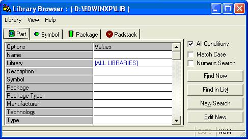
open Library Browser.
2. Select the library - All Libraries, Project Library (libraries loaded or present in the opened Project) or other libraries (e.g. other Libraries - 54TTL.PART)
3. Set the necessary options. Check All Conditions, to narrow the search taking into consideration all information entered for the options. If necessary check Match Case.
4. Click Find Now button. The system now searches the component(s) in the selected library with the options set and displays the result in the search list.
5. Select the component(s) from the search list and drag & drop into the Schematic / layout editor or Send to Schematic/Layout.
Fig.3.27 Library Browser
How to Add Components?
Components may be added to the current project without activating Library Browser/Explorer.
Components in the custom libraries will be pulled out only if they are placed higher up in the search sequence. Else they will be overridden by the first available component in the search list.
Steps:
i. Click on the option tool Add components by name, from Add
components to the circuit function tool of Schematic or layout Editor, to popup a textbox.
.
Fig.3.28ii. Type in the name of the component to be added to the project.
iii. Click on Accept to get an image of the component tagged to the cursor.
iv. Click anywhere on the workspace to place it.
On each click on the workspace the component gets repeated until the Esc key is pressed. To position the component at a particular point on workspace, give the corresponding XY coordinate along with the component name.
EDSpice Symbol Editor
In order to simulate a schematic component using EDSpice Simulator, its symbol must be associated with one of the available EDSpice circuit elements or with the subcircuit from EDSpice Subcircuits Library. This application facilitates the association of symbols in Symbol library to the available EDSpice circuit elements or subcircuits and define the component parameters. EDSpice Simulation references may be added to parts or the already assigned ones may be changed using this module.
Starting EDSpice Symbol Editor
Click on the task
Library in the Project Explorer and adopt either of the following methods:
- Right click on
Library and then select the function
EDSpice Symbol Library Editor
- Select
EDSpice Symbol Library Editor from the task list or from the task toolbar.
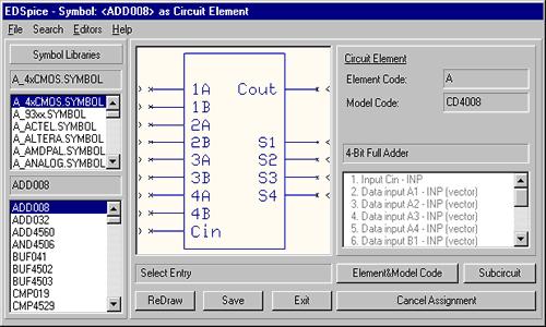
The EDSpice Symbol Editor window opens as shown Fig.3.29
Fig.3.29 EDSpice Symbol Editor
The scale of the displayed symbol may be changed by pressing the hot key combination Shift U (Zoom Up) or Shift D (Zoom Down). The picture may be panned with center at current cursor position by clicking the right mouse button. The button when clicked redraws the symbol in current scale with entry #1 in the center of the picture.
The required part/ symbol may be selected from their respective libraries or searched using the menu item Search. Either the part or the symbol may be searched according to the mode selected from the menu Editors.
Editors <= Symbol
The selected/searched symbol gets displayed in the display area. This symbol may be assigned element and model code or a subcircuit.
How to assign element and model code/subcircuit to the symbol
| 1. | Select the appropriate circuit element from the list and press SUBCIRCUIT. |
To assign subcircuit, if 'Add family prefix' is checked, the prefix gets added to the symbol
| 2. | Assign element nodes to the appropriate entries of the symbol. When a circuit element has been selected, the list of nodes, as expected by EDSpice is displayed. The sequence of operations is as follows: |
||||
|
|||||
| The same operation must be repeated for all entries in the symbol. | |||||
Editors <= Part
The purpose of this mode is to set the Simulation Reference to the parts. In this mode, a new window overlaps the previous one and has two list boxes, one listing the part libraries in the selected library path and the other listing the parts in the selected *.PART library.
If the symbol associated with the part highlighted has a model code assigned to it, a list of model library names with the same prefix as the assigned one gets displayed in a list box to the right of the window. If the symbol has a subcircuit assigned to it, a list of library subcircuits with the same number of nodes as the assigned one is displayed.
EDSpice Simulation References are assigned to parts and not to symbols. Hence it should be noted that only those components created as parts would be properly attached to the subcircuit/ model parameters referred to by the Simulation Reference. The component has to be packaged before pre-processing by EDSpice
While preprocessing the circuit in EDSpice simulator, the subcircuit/ (model code) assigned to the part overrides the default assignment made for the symbol. The specific subcircuit assignments made to symbols, if any, has the highest priority. Users may create their own model/ subcircuit families and attach simulation reference to Parts adhering to the above mentioned regulations. Note that no subdirectory is allowed in the Model Parameter Library EDWinXP\EDS_MOD. Also, Family subdirectories for subcircuit should be of one level in EDWinXP\ EDS_SBK directory, e.g. the file structure shown in adjacent figure is invalid.
Field Editor
Field editor window lists all the components available in the Library. The main function of the utility is to maintain the existing libraries. Main purposes of this module are:
- To convert older libraries created in EDWin16 and EDWin32 to be compatible to EDWinXP format (Refer Chapter 2-Conversion Manager Page :39)
- Maintaining and updating the already existing libraries
- Creation of special parts
- Adding thermal parameters
- Upgrade old Package name to new Package name of a PART. E.g. DIP14 to DIP14/300. Here the physical attribute of the package is not affected.
Fig.3.30 Field editorStarting Field Editor:
This module may be invoked from Project Explorer in the following ways
- Right click Library
and select
Field Editor from the list.
- Select
Field Editor from the task list or from the task toolbar.
The window of Field editor is shown in Fig.3.30.
| File File menu provides a list of different library groups, each of which may be selected to obtain detailed information of components belonging to that category. There are options for setting the library path and refreshing the listed library on the left side pane. |
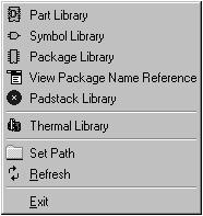
Fig.3.31 |
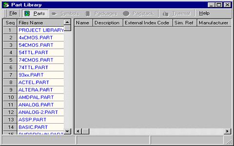
Parts
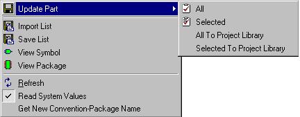
Selecting this option displays Field editor window with part tab activated. The window provides information about all parts available in the package. Details such as name, full name, External index code, simulation references, manufacturer, different types, technology, package type, simcode, element code/model or subcircuit/ variant, symbol name and package name of each of the parts are listed here. Double click on any of the listed part library on the left side pane to get property fields of different parts belonging to that group. Right clicking on any of its fields pops up a floating menu as shown below, this gives the option for updating the records, importing/saving it and for viewing separately the symbol and package. It also allows reading the system values of listed part fields.
Fig.3.32Update part All/Selected
Allows to update the records of either a selected part or all listed parts. Any modification done on this may be saved. Click on the required columns of any of the part’s record for editing the values. User may either directly type in the values or it may be selected from a given browse list. Non editable fields are indicated by a light yellow color. If updating is tried on system libraries, the system issues an appropriate error message. Any custom libraries may be chosen for saving the updated information.
Import List
Allows loading *.DST files. Select this option to pop up a dialog box. On giving the necessary path the saved list gets imported.
*.DST files contain information of the parts saved previously.Save List
Allows saving any of the listed part’s fields information in the format (*.DST). Select this option to pop up a dialog box. On giving the necessary path the item gets saved as *.DST file.
View symbol
Using this option, symbol may be viewed separately in a viewer window.
View package
Using this option, package may be viewed separately in a viewer window.
Refresh
This option refreshes the displayed list of parts. If a record of any of the selected part is changed, the list on the right side pane will display the changed fields. Original fields (that which is stored in the system libraries) may be retrieved with this option.
Read System values
Selecting this option loads all the internal information about the part, which has been already specified. These system values cannot be changed. Disabling this option enhances the speed of loading libraries.
After enabling Read System values, it is necessary to Refresh the window.
Get New Convention Package Name
When a Part library is selected from the Field editor window the package name displayed in the right side panel is the currently used name in the new version. But these names are slightly different from the convention names in the older version. Hence, for getting the old convention name corresponding to each package, this option has to be enabled. By selecting this option a window pops up displaying the packages not having their standard names. In the right side pane a new field displaying the old convention name will also be included. This option does not appear for Project Library as the physical attributes might be changed.
By selecting project library from the list, the right click pop up menu obtained will not be the same as above. It includes two more options as shown in Fig.3.32.
All to project library
By choosing this option all the listed component’s field gets updated to the project library.
Selected to project library
This option allows to update only the selected part’s field to the project library.
View symbol and view package (for the project library) options will only be active if there is the required information in the corresponding columns. By selecting any of the part, it’s symbol and package may be viewed.
Symbol Selecting this option displays Field editor window with Symbol tab activated.
The window lists all the symbols available in the package. Double click
on any of the listed symbol libraries in the left pane to get records
of symbols belonging to that group. The different fields may be edited
and the changed symbol record may be updated by selecting required options
from the floating list obtained on right click. |
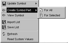 Fig.3.33 |
This module allows special creation of parts without an associated package. These are mainly used for simulation purposes. Right clicking on any of its listed records pops up a floating menu as shown below, which gives the option for updating the elements, importing/saving it and for viewing separately the symbol. It also allows reading the system values of listed items and refreshing the list.
Update symbols
Allows to update the records of either a selected symbol or all listed symbols. Any modification done on the listed fields may be saved using this. Click on the required columns for editing the fields. User may either directly type in the values or it may be selected from a given browse list Non editable properties are indicated by a light yellow color. If updating is tried on system libraries, the system issues an appropriate error message. Any custom libraries may be chosen for updating the symbols.Create symbol part
Allows creating special parts without an associated package. Either a selected symbol or the whole list may be created like this special part. These are mainly used for simulation purposes. Selecting this option pops up a save dialog box in which a custom library may be chosen for saving the special parts. These special parts may be viewed by selecting the PART tab from the main menu and double clicking on the required part library. The special part name has the prefix SMB_ added to the name of the original part.View symbol
Using this option, symbol may be viewed separately in a viewer window.Import List
Allows loading *.SST files. Select this option to pop up a dialog box. On giving the necessary path saved list gets loaded.
*.SST files contain information of the symbols saved previously.Save List
Allows saving the listed symbol fields information in the *.SST format. Select this option to pop up a dialog box. On giving the necessary path the selected symbol library fields gets saved.Refresh
This option refreshes the displayed list of items. If properties of any of the loaded items are changed, the list on the right side pane will display the changed properties. Original properties (that which is stored in the system libraries) may be retrieved with this option.Read System values
Selecting this option loads all the internal information about the symbols which has been already specified. These system values cannot be changed. Disabling this option enhances the speed of loading libraries.
After enabling Read System values, it is necessary to Refresh the window
Package Selecting this option displays Field editor window with Package tab activated. The window lists all the packages available. Double click on the required package library in the left pane to get details of all packages belonging to that group. The different parameter fields may be edited and the changed package record can be updated by selecting required options from the floating list obtained on right click. |
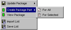 Fig.3.34 |
This module allows special creation of parts without an associated symbol. There are options for viewing the packages separately and for importing/ saving it. Pop up list obtained on right click is as shown in Fig.3.34.
Update package
Allows to update either a selected package field or fields of all the listed packages in the selected library. Any modification done on the listed property fields may be saved using this. Click on the required columns for editing the values. User may either directly type in the values or it may be selected from a given browse list. If updating is tried on system libraries, the system issues an appropriate error message. By this users are prevented from tampering the system libraries. Any custom libraries may be chosen for updating the packages.Create package part
This option allows special creation of parts without an associated symbol. This is mainly be used for creating mounting devices. Selecting this option pops up a save dialog box in which a custom library may be chosen for saving the special parts. These special parts may be viewed by selecting the PART tab from the main menu and double clicking on the required part library. The special part name has the prefix PKG_ added to the name of the original part.View package
Using this option, package of the selected part may be viewed separately in a viewer window.Import List
Allows loading *.LST files. Select this option to popup a window, in which the required path may be browsed to import that item.*.LST files contain information of the package saved previously.Save List
Allows saving the listed Package fields information in the *.LST extension. Select this option to popup a dialog box and enter the required path to save the list.View Package name reference
Selecting this option opens a window "Info", which displays the names of the packages in accordance with the old and new conventions. Corresponding to each old convention package name, the new name is displayed.
Padstack Selecting this option displays Field editor window with padstack tab activated. The window lists all the padstacks available. Double click required padstack library in the left pane to get details of padstacks belonging to that group. The different parameter fields may be edited and the changed padstack record may be updated by selecting required options either from the main menu or from the floating list obtained on right click. There are also options for viewing padstacks separately and importing/saving it. |
|
Update padstack
Allows to update either a selected padstack field or fields of all the listed padstacks. Any modification done on the listed property fields may be saved using this. Click on the required columns for editing the values. User may either directly type in the values or it may be selected from a given browse list. If updating is tried on system libraries, the system issues an appropriate error message. Any custom libraries may be chosen for updating the fields.Import list
Allows importing *.PST files. Select this option to pop up a window in which the required path may be entered for loading the saved list.*.PST files contain information of the padstack saved previously.Padstack Save list
Allows saving the listed Padstack fields information in the *.PST extension. Select this option to popup a window. Enter the required path. The list is saved in that location.View padstack
Allows viewing pads in a separate viewer windowThermal parameters
Selecting this option displays Field editor window with thermal tab activated. The window lists all thermal libraries available. The different fields of thermal parameters may be re-edited from this window. The changes may be saved in a custom library other than the system libraries. If modification is attempted on the existing system libraries, the system will issue an appropriate error message. Double click on any of the listed thermal libraries to display the corresponding thermal parameters associated with each component. Right clicking on any of the listed component in the right pane pops up a list that allows to update, save and load items. This pop up list is shown in Fig.3.36.
Fig.3.36Update Thermal Values
Any of the listed component’s thermal parameter fields may be edited by clicking on the corresponding columns. User may either directly type in the values or it may be selected from a given browse list. These changed fields may be updated by selecting this option. Updating of the changed fields may done on any of the custom libraries other than the system library. If updating is tried on system libraries, the system issues an appropriate error message. There is option for updating either a selected or all the listed component thermal parameter fields.Import list
Allows loading the *.DAT files. Select this option to pop up a dialog box in which required path may be given for loading the saved list.Save list
Allows saving the selected component’s thermal fields in the ` *.DAT format.
Set path
Allows to set the path of required libraries.
Refresh.
This option refreshes the listed libraries by reloading it from the disk.
Exit
Allows to exit from this module.
 How
to pass older (EDWin 16 and EDWin32) library components through Field editor?
1. Using Conversion manager convert EDWin 16 bit libraries. EDWin32 libraries
need not be converted.
2. Open Field editor, and choose the path where library is residing.
3. Double click on the required library and on right pane, right click and enable
option Read System Values and Refresh.
4. Now these libraries may be added with required information and updated.
 How
to Import older libraries and databases (projects)?
- Using EDWin 16 libraries and databases
All EDWin 16 bit databases and libraries should be converted to the new format using Conversion Manager (exactly as in EDWin 32).A library element in the new format contains additional fields for storing cross-references and in case of parts even thermal parameters These cross-references are not needed for proper functioning of the system but are useful for searching and browsing. Since this information cannot be reconstructed automatically during conversion, a special program called Field Editor has been provided. Certain cross references required for proper functioning of Library Browser and Library Explorer will be updated automatically when library file is passed through Field Editor. For example: in EDWin 16 thermal parameters were kept in separate files (.DAT/ .TAL). Now all this data is stored within the respective Parts. Field Editor also enables to add other necessary information (manufacturer name, type etc) in manual edit mode.
In the latest version, when you try to save old DEVICES or PARTS taken from old DATABASES, it is required that you have to save the corresponding symbols and packages used by the Parts into User Libraries (and of course subsequently included those files into the Search Sequence).
-
Using EDWin 32 Libraries and databases.
All EDWin 32 libraries and databases are upward compatible and for viewing with the latest version NEED NOT be converted.Although, for using the libraries, it is required to pass the library files through Field Editor.
CAUTION:
Any attempt (even for browsing using Library Explorer or Browser) to access EDWin32 libraries from the latest version causes permanent change of format. EDWin 32 libraries and databases once used with the new package cannot be used with EDWin32.
PLEASE ALWAYS USE SEPARATE COPIES OF LIBRARY AND DATABASE FILES FOR EDWIN 32
AND NEW VERSION.
THE PATHS FOR LIBRARY AND DATABASE FILES OF EDWIN 32 AND THE NEW VERSION MUST
NOT BE SAME...
In the latest version, when you try to save old DEVICES or PARTS taken from old DATABASES, it is required that you have to save the corresponding symbols and packages used by the Parts into User Libraries (and of course subsequently included those files into the Search Sequence).
