Mixed Mode Simulator
Mixed Mode Simulator, the system's native circuit level analyzer test the functioning of the circuit .This Simulator supports TD, DC, AC Parameter sweep, Fourier, Monte Carlo and Sensitivity analyses of analog, digital, and mixed-signal circuits.
Steps for Mixed Mode Simulation
Create/Load the Project
You can create a new project by using EDWinXP –Main Menu File/New Project. Please Refer Chapter 4 to know more about project creation.
Or Load the existing project using EDWinXP –Main Menu File/Open Project.
Invoking the Mixed Mode Simulator
Mixed Mode Simulator can be invoked from Schematic Editor /Preferences/ Mixed Mode Simulator.
| Preprocess the circuit
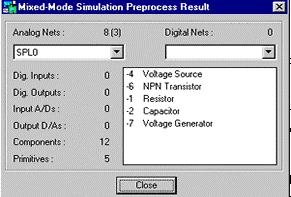
You can evoke preprocessing from Simulation Menu. The simulator analyzes the schematic first and checks for the simulation function. It generates the data along with the statistics of the circuit. Data includes the number of digital and analog nets, list of symbols, which may be simulated along with their simulation functions, number of digital inputs and outputs, number of A/D input/ outputs. This is presented as a dialog box. Observe that the analog primitives are assigned negative simulation function. |
Click the Close button to close this dialog box. The simulator is now ready for making further analysis on the circuit. (Refer Fig.6.1)
Any change
in the circuit element values or topology gets implemented only if the preprocess
is invoked. Preprocessing the circuit resets the values set.
Set element value
Before executing the analysis, set the circuit element values.
Select the option tool
Change Simulation Parameters from the function tool Component Properties
in
Components or
Instruments Toolbar and click on the component.
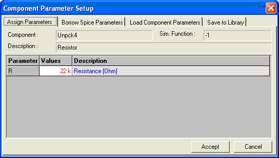
Fig 6.2: Component Parameter setup window
For e.g.: Component Parameter setup window for a resistor is as shown in the figure
Now edit the default value by clicking the particular cell. In this way the parameters for each element needs to be assigned.
Place test points/ waveform markers
The analysis result may be viewed at all element nodes by placing
appropriate
Test points/
Set Waveform Contents (if graphical output is required). After selecting
the suitable test points, click on the connection/ pin to assign the test point.
Move the small outline rectangle to the desired position to place the test points
(Refer Fig.6.3).
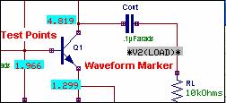
Fig 6.3
Set simulation limits
The default simulation parameters like temperature, iteration limits, and minimum displayable units may be reset using Setup Simulation Parameters. This window can be invoked from Analysis/General Settings.
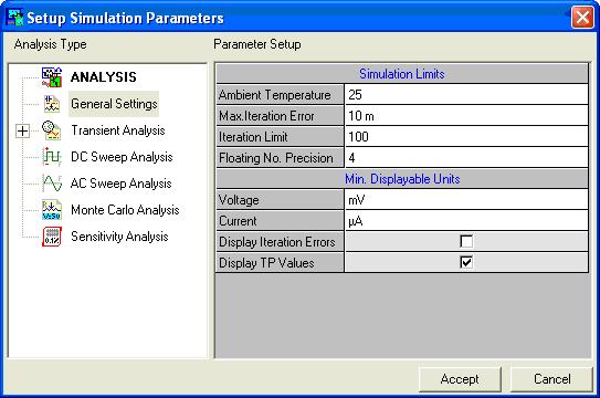
Fig 6.4: General settings
Execute analysis
Invoke Analysis from the Simulation Menu and choose the required analysis. Set the parameters and click on Accept button to execute the Analysis.
Tips:
Check Display waveform option to view the result
immediately.
Types of Analysis Supported by Mixed Mode Simulator
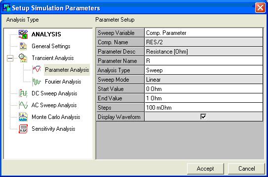
Fig 6.5
- Bias Point Calculation
- Transient Analysis
- Parameter Analysis
- Fourier Analysis
- DC Sweep Analysis
- AC Sweep Analysis
- Monte Carlo Analysis
- Sensitivity Analysis
Bias Point Calculation
Please refer sample project (EDWinXP/Job/ MIXMODE_EDSPICE) Amplif.EPB
Steps:
1. Right click and select the
Test Points function tool. Select the
Voltage TP and place the test points at the base, collector and emitter
of the transistor 2N3227 (Refer Fig. 6.6).
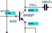
Fig. 6.6
2. To review the 2N3227 transistor parameters, select the function
tool
Component Properties and then the option tool Change Simulation Parameter.
Click on the transistor to view the component Parameter Setup of the transistor.
These parameters can be modified. Click CANCEL to exit the dialog box
without effecting change and ACCEPT button for the changes to come into
effect.
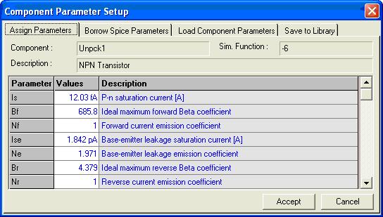
Fig. 6.7
3. After setting the parameters of the circuit, select Simulation / Analysis. A window Setup Simulation Parameters pops up as shown in the figure.
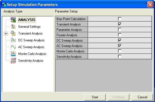
Fig 6.8
Set the parameters by selecting GENERAL SETTINGS from the tree view on
the left side of the window. Click Accept button to accept the changes
and to automatically switch to Analysis option. Select Bias Point Calculation
and click the START button.
You can observe that the node voltages are displayed at the
locations where test points were placed. From this we will observe that the
operating point of the transistor is found to be near the saturation region.
For more details, you can check its Base and Collector currents. Right click
and select
Current TP option tool from the function tools of
Test point. Click on transistor base and collector pins to place
the Current Test point Display Box.
It is necessary to run Bias Point analysis before any other analysis to set
the values of the test points placed.
Transient analysis
In the Transient analysis, we will study the performance of the circuit in time frame.
For example, in AMPLIF.EPB the amplifier is fed with an input signal that varies with time in specified manner. Transient Analysis is used to view the input and output with respect to time.
We have analyzed the amplifier small signal properties. At 10 kHz, amplification is 40dB (output amplitude is about 90 times greater than input signal), this means that we can apply max. of about 50mV on input without distortion:
1. We will now define the amplitude of the generator signal. Right click and select the function tool
Component Properties and then the option tool
Change Simulation Parameter, click the input generator VGEN, the component parameter set up window appears as shown in Fig. 6-9.

Fig. 6.9
2. The Voltage Generator is in the SINE mode and produces 10mV, 10kHz signal. This would be amplified without distortion. As you found from AC Sweep analysis, the maximum amplitude that may be specified was about 50 mV. Click the Accept button to save the changes.
3. Right click and select theDelete tool and delete all previously used Waveform Test points.
4. Right click and select the
Voltage Waveform option tool from the function tool
Set Waveform Contents and define new Voltage test points on the nets, on generator input (between VGEN and resistance RG), on transistor Base, on transistor Collector and on amplifier load (between C2 and RL).
5. Select theCurrent Waveform option tool from the function tool
Set Waveform Contents and define new Current test points on the pins: generator “-” pin, transistor collector pin, load resistor RL (upper pin).
6. Click Analysis in the main menu. A window Setup Simulation Parameters opens with the option Analysis being highlighted Set the parameters by selecting GENERAL SETTINGS.
7. Select Transient Analysis. Specify the timing parameter. Set the Analog Sim. Step time to 1 microsecond, Simulation Time Limit to 200 micro second (two generator periods). Initialize LC parameter should be set to Solve (Refer fig. 6-10).
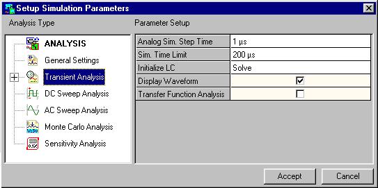
Fig. 6.10
8. Click the ACCEPT button which automatically switches Analysis option. Here, check Transient Analysis and click START button. The result is displayed as a diagram if Display Waveform is checked.
9. We may change the Generator parameter Ao from 10mV to 100mV and rerun the Transient Analysis. You can view some distortion in the output waveform.
10. Reset the value of Ao to 10mV.
Tips:
The result of an analysis can also be viewed in text format (decimal/hexadecimal/binary)
with the Logic Analyzer (Simulation/Run Transient Analysis (Logic Analyzer)
.The output at any point of time during the simulation can be obtained in word
format using this application.
Transient Analysis on Digital circuits
From the File menu of the Project Explorer, select Open Project/ PCB Layout folder and then open Counter.EPB from the file list.
Before starting the Transient Analysis, the circuit state must be initialized. Analog part of the circuit has one state variable: voltage on the capacitor C. We may assume that it starts from the zero value (the power-up condition). This may be achieved by the proper setting of the Transient Analysis/ Initialize LC option in the Setup Simulation Parameters dialog box invoked from the Analysis menu.
1. Initialization of the digital part of the circuit is essential as outputs of the inverters, and output state of the D Flip-flop must be considered. We have to input a Clock pulse to analyze the working of the circuit.
2. Right click and select the option tool
Clock Generator from the function tool
Preset Logic State and click on the 7404,1 (U1) and enter the generator string value of (L10us,H10us). This indicates a continuous clock pulse having a 10µs Low and 10µs High pulse width.
3. Enter 5V to the Voltage source from the
Change Simulation Parameters tool and clicking on the Voltage Source.
4. Place Logic state marker on the input node of U1 and on output nodes (Q) of all D-Flip flops using the option tool
Logic Waveform enabled from the function tool
Set Waveform Contents
5. Click Analysis in the main menu. A window Setup Simulation Parameters opens with the option Analysis being highlighted on the left side of the window by default. Set the parameters by selecting GENERAL SETTINGS from the tree view on the left side of the window. Select Transient Analysis and set Analog Sim. Step Time to 10 microseconds. Set Simulation Time Limit to 500 microseconds. Set Initialize LC to Solve. Click the ACCEPT button to automatically switch to the Analysis option and select the START button to begin the analysis (Refer Fig. 6.11).

Fig. 6.11
6. After the analysis is completed, the result is displayed as a diagram if Display Waveform is checked. Value of the Analog Simulation Step Time defines time step used in the analog integration process resolving the capacitor voltage. It also defines sampling rate of analog data output to the diagram display module. The shorter the Analog Sim. Step Time, better is the accuracy of analog integration and density of analog graphic results obtained.
Tips:
To view the transient analog /digital response of any node or net in the circuit.
Select Instant analog probe or Instant digital probe from Instruments/Instant
Probes and click on the required node/net. The response that appears in the
waveform viewer will be node current or net voltage depending on whether node
or net is selected.
Parameter Analysis
This analysis mode allows studying the effect of variation of component parameters on the circuit. This is helpful in setting up the best operating conditions for the design, before detailed functional analysis is made.
1. Right click and select the function tool
Set Waveform Contents and then the
Voltage Waveform option tool and define new Voltage test points on the nets, on generator input (between VGEN and resistance RG), on Collector terminal of the transistor and on amplifier load (between C2 and RL).
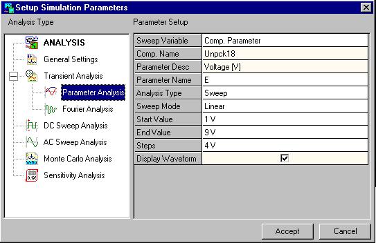
Fig. 6.12
2. Click Analysis in the main menu. A window Setup Simulation Parameters opens with the option Analysis being highlighted on the left side of the window by default. Set the parameters by selecting GENERAL SETTINGS from the tree view on the left side of the window. Now, select the Parameter Analysis option (Refer Fig. 6-12).
3. Select the Sweep Variable as ‘Comp. Parameter’. Move the cursor over Voltage Source and click the left mouse button. The selected component name and parameter name appears in the dialog box. If it has only one parameter, then it is automatically selected. If you have more parameters, you will have to specify the parameter of the component, e.g., a transistor, from the drop down ‘Parameter Name’.
4. Set the values for the following parameter as shown below.
Start Value .........1V
End Value ..........9V
Step ...................4V5. Click ACCEPT button to automatically switch to Analysis option. Check Parameter Analysis check box. Now click START button for analysis to take place. The results may be viewed in the Waveform Viewer and the most suitable parameter value may be obtained.
Fourier Analysis
This analysis is used to calculate the total harmonic distortion of analog waveforms generated on conducting transient analysis.
1. We will check the harmonics of the waveform generated on conducting Transient analysis of AMPLIF.EPB.
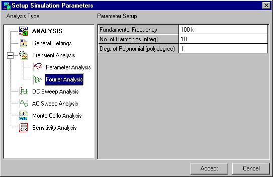
Fig. 6.13
2. Select Analysis from the main menu to open Setup Simulation Parameter with the option Analysis being highlighted on the left side of the window by default. Set the general parameters and select Fourier Analysis from the tree view or obtained on right clicking Analysis.
3. The parameters to be set are the fundamental frequency of the waveform whose distortion is being computed. Set it as 100KHz. No. of harmonics as 10 and the degree of polynomial to be 1 (Refer Fig. 6.13).
4. After setting these parameters, click the ACCEPT button to accept the parameters and automatically switch to Analysis option. Check Fourier analysis. The START button executes the analysis and displays the process in the Progress bar.
5. The results are displayed in a text format.
DC Sweep Analysis
DC Sweep Analysis: Bias Point Setup
Let us examine the effect of the circuit AMPLIF.EPB modifying the value of RB2 on the operating condition of the circuit. We will vary the value of RB2 from say, 5K to 20K in steps of 0.5K and observe the circuit operating parameters. We would like to present the results in a graphical form to assess the correct value for RB2. The parameters of concern for this analysis are Vce, Ib and Ic. As we need graphical representation, we will have to define these points.
1. Right click and select the
Voltage Waveform option tool from the function tool
Set Waveform Contents. Define Voltage Waveform Marker for Collector voltage by clicking on the wire connected to the transistor Collector pin. In the same way, define for Emitter voltage.
2. Right click and select the
Current Waveform option tool from the function tool
Set Waveform Contents. Define Current Waveform Marker for Base current by clicking on the transistor Base pin. In the same way, define for Collector current.
3. Click Analysis in the main menu. A window Setup Simulation Parameters opens with the option Analysis being highlighted on the left side of the window by default. Set the parameters by selecting GENERAL SETTINGS from the tree view on the left side of the window. Now, select the DC Sweep Analysis option (Refer Fig. 6.14).
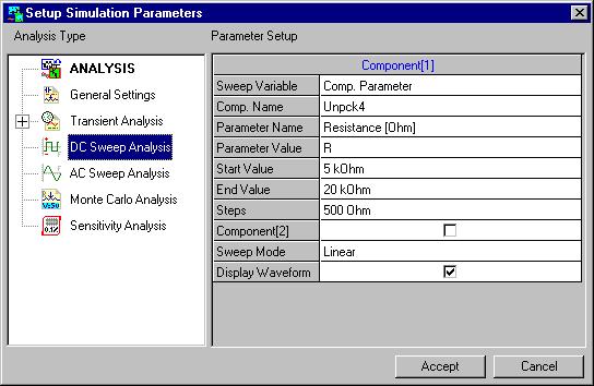
Fig. 6.14
4. We will first select the Sweep Variable as Comp. Parameter in this dialog box. Move the cursor over the resistor RB2 and click the left mouse button. The selected component name and parameter name appears in the dialog box. Selected resistor has only one parameter, and is automatically selected. If we have more parameters, we will have to specify the parameter of the component, e.g., a transistor, from the drop down ‘Parameter Value’. We may conduct the analysis when the parameter of one circuit element is varied keeping the parameter of another circuit element constant, through out a range of values. In that case, check the check box Component (2) and set its parameters.
5. We will now set the sweep limits for RB2, enter 5k in the Start value box, and 20k in the End value edit box. As the range is limited for sweep, we can choose Linear and enter 0.5k in the Step edit box. This completes the parameter setting. We can enable the check box next to Display waveform, if we want the system to automatically pop up the display waveform. We will not select this for the current exercise. Click ACCEPT button to automatically switch to Analysis option. Check DC Sweep Analysis check box. Now click START button for analysis to take place.
6. During the simulation, we may observe the results as they occur in each step. To choose the best bias point result depended on the setting of the resistor RB2, we will use the graphical results of the simulation.
7. The Waveform Viewer (enabled automatically if Display waveform is checked.) application window appears showing four curves as results of the analysis. These curves show the waveforms defined earlier, viz. V1 (Collector), V2 (Emitter), I1 (Base) and I2 (Collector). From these waveforms, we must solve a little problem. Find the RB2 value for which Ic/Ib = Beta (approx.) and Vc-Ve is about half of Vcc-Ve.
8. Close the Waveform Viewer.
9. We will now modify the value of RB2 to the value arrived at after the analysis. Select the function tool
Component Properties and then select the option tool
Change Simulation Parameter to update the component value for RB2. Click the left mouse button on the RB2 resistor. Click the cell under the value column. Enter the new value (11kO into the editable text box at the current location) in the appeared Assign Parameter For dialog box (Refer Fig. 6-15).
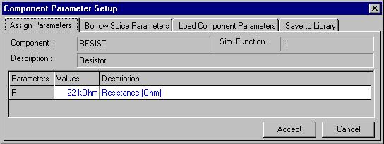
Fig. 6.15
10. Click the ACCEPT button. We will observe the new value for RB2 on the simulation screen.
11. We will recompute the bias points to ensure that the transistor operating condition is just right. From main menu choose Analysis. Check DC Sweep Analysis check box. Now click START button for analysis to take place. Verify the results.
DC Sweep Analysis: Transistor Beta Bf
We will try out DC Sweep analysis for checking circuit sensitivity when the transistor parameter Beta (Bf) changes from 100 to 400.
1. Click Analysis in the main menu. A window Setup Simulation Parameters opens with the option Analysis being highlighted on the left side of the window by default. Set the parameters by selecting GENERAL SETTINGS from the tree view on the left side of the window. Now, select the DC Sweep Analysis option. Move the cursor over the transistor and click the left mouse button.
2. As the transistor has more than one parameter, all parameters are listed in a drop down defined for the component. Here, select the Bf parameter from the Parameter Value drop down in the Setup Simulation Parameters dialog box.
3. Define the sweep limits as 100 for the Start value edit box and 400 for the End value. Select the Sweep mode to be Linear and enter 20 in the Step cell. Click the ACCEPT button.
4. In the Progress display area, current iteration status (iteration number and voltage errors) is displayed continuously. We may disable this option and speed up the simulation. For this, select the General Settings option in the Setup Simulation Parameters dialog box that appears when Analysis is clicked in the main menu. Change selection of the check box named Display Iteration Errors. Click the ACCEPT button.
5. We may also disable the Display TP values check box in General Setting’s option to obtain the fastest simulation run. Results may be reviewed in the Waveform Viewer only.
DC Sweep Analysis: Operating Temperature
We may also sweep the ambient temperature and observe the circuit response:
1. Click Analysis in the main menu. A window Setup Simulation Parameters opens with the option Analysis being highlighted on the left side of the window by default. Set the parameters by selecting GENERAL SETTINGS from the tree view on the left side of the window. Now, select the DC Sweep Analysis option.
2. Select the Sweep Variable as Temperature.
3. Define the sweep limits as -30 for the Start value edit box and 100 for the End value. Select the Sweep Mode to be Linear and enter 5 in the Step box. Click the ACCEPT button.
4. Observe the results in the Waveform Viewer, after checking Display Waveform check box in the Setup Simulation Parameters dialog box.
AC Sweep Analysis
The circuit operating parameters have all been stabilized for the circuit AMPLIF.EPB and set after the DC sweep analysis. Now we may calculate the small-signal frequency response of the circuit assuming its current biasing. We will not define any AC parameters for the active components like transistor - the Simulator assumes their values calculated internally from the nonlinear transistor model using its operating point.
1. Before any further analysis is performed, compute the operating point again, using Analysis menu
2. We will now have to define the AC Analysis input points. Right click and select the
AC IN+ option tool from the function tool
Set Reference Points. Click the left mouse button at the “+” terminal of the Generator. We will see a text “IN+”, position this AC Input test point.
3. To define the AC Analysis output points, right click and select the
AC OUT+ option tool from the function tool
Set Reference Points. Click the left mouse button on the net connected between C2 and RL. We will see a text “OUT+”, position this AC output test point.
4. The AC test points IN- and OUT-, for AC input and output are by default assigned to ground net SPL0 and we need not define them except for special cases.
5. We will now have to define the frequency sweep parameters. Click Analysis in the main menu. A window Setup Simulation Parameters opens with the option Analysis being highlighted on the left side of the window by default. Set the parameters by selecting GENERAL SETTINGS from the tree view on the left side of the window. Now, select the AC Sweep Analysis option
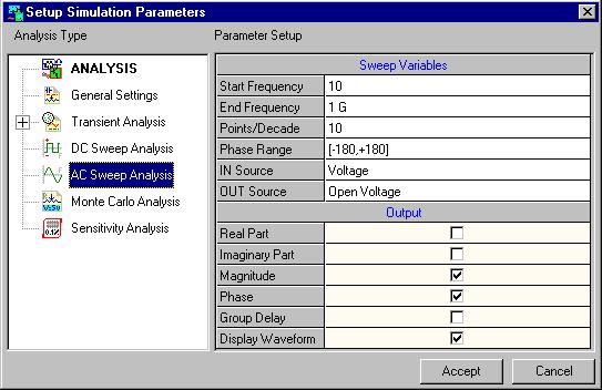
Fig. 6.16
Set the values for the following parameter as shown below.
Start Frequency End Frequency Points per Decade Range of Phase IN source OUT variable Output |
10 Hz 1 GHz 10 [-180°, +180°] Voltage Open voltage Magnitude,Phase, Group Delay. |
6. We will observe that the AC simulation will analyze the circuit response for a frequency sweep from 10 Hz to 1 GHz (8 decades) with 10 points per decade - total 81 points. Phase shift is calculated within the range from -180° to +180°. An AC voltage input source is placed between IN+ and IN- net. An AC voltage is measured on the opened OUT+ and OUT- nets. The ratio Vout / Vin will be an output that is shown in three forms: magnitude, phase and group delay.
7. Click ACCEPT button to automatically switch to Analysis option. Check AC Sweep Analysis check box. Now click START button for AC Simulation Pass to take place.
8. If Display Waveform is checked in the above dialog box, the output is displayed in the Waveform Viewer and the three curves depict the graphical dependency of the calculated Gain, Phase Shift and Group Delay from the frequency parameter. From this, we see that the lower unity-gain frequency is about 60 Hz, upper unity-gain frequency is about 50 MHz. Middle-frequency gain is about 40 dB.
We will save the results by Selecting File | Save in the Waveform Viewer menu. Specify the name of the file and click OK. Exit from the Waveform Viewer.
We can now test the circuit AC characteristics for another bias point. For example, with the RB2 set to its original value 20k ohms do the following.
1. Right click and select the
Component Properties and then select the option tool
Change Simulation Parameter and set RB2 resistor to 20k value.
2. Click Analysis in the main menu and select the Analysis from the Setup Simulation Parameters dialog box that appears. Enable the Bias Point Calculation check box in order to recompute the bias point for the design.
3. Enable AC Sweep Analysis check box after selecting the Analysis option in the Setup Simulation Parameters dialog box. Click the ACCEPT button to start the AC analysis.
4. Display the AC Sweep diagram.
5. We see that unity-gain frequencies are now 180 Hz and 500 kHz, and the maximal gain is now about 24 dB. The original bias point gives a poor AC circuit response.
Monte Carlo Analysis
It is used to calculate accurate component parameter values for a given output at a given instant of time. We will study the performance of the circuit AMPLIF.EPB.
1. Right click and select the
Monte Carlo Voltage option tool from the function tool
Set Reference Points. Define the reference point by clicking on the wire connected to the transistor Collector pin.
2. Click Analysis in the main menu. A window Setup Simulation Parameters opens with the option Analysis being highlighted on the left side of the window by default. Set the parameters by selecting GENERAL SETTINGS from the tree view on the left side of the window. Now, select the Monte Carlo Analysis option.
3. We will select the Component RB1. Move the cursor over the resistor RB1 and click the left mouse button. The selected component name and parameter name appears in the dialog box. Selected resistor has only one parameter, and is automatically selected. If we have more parameters, we will have to specify the parameter of the component, e.g., a transistor, from the drop down ‘Parameter Value’. We may conduct the analysis when the parameter of one circuit element is varied keeping the parameter of another circuit element constant, through out a range of values. In that case, check the check box Component (2) and set its parameters.
4. Set the Tolerance to be 10% and No. of samples 10. Tolerance specifies the percentage range of variation of component parameters. No. of Samples specifies the number of iterations within the output range for which analysis is to be carried out. Time specifies an instant of time at which the accurate parameter value is to be calculated for obtaining the specified output. Set it as 10ms (Refer Fig. 6-17).
5. Click ACCEPT button to automatically switch to Analysis option. Check Monte Carlo Analysis check box. Now click START button for analysis to take place.
6. The results are displayed in a text file.
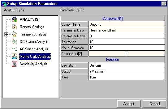
Fig. 6-17
Sensitivity Analysis
It is used to calculate the component that is most sensitive to an output reference point. Please refer AMPLIF.EPB to study the performance of the circuit.
1. Right click and select the
Sensitivity Voltage option tool from the function tool
Set Reference Points. Define the reference point by clicking on the wire connected to the transistor Collector pin.
2. Click Analysis in the main menu. A window Setup Simulation Parameters opens with the option Analysis being highlighted on the left side of the window by default. Set the parameters by selecting GENERAL SETTINGS from the tree view on the left side of the window. Now, select the Sensitivity Analysis option (Refer Fig.6-18).
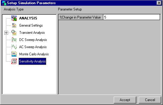
Fig. 6.18
3. Specify a 5% of tolerance for which the analysis is to be carried out. This is the common tolerance value for all parameters of all components.
4. Click ACCEPT button to automatically switch to Analysis option. Check Sensitivity Analysis check box. Now click START button for analysis to take place.
5. The results are displayed in a text file. The most sensitive component and its parameter is listed as the last line of the text file.
Tips: Use Multimeter from Instruments/ Test Points
and click on the net or node to view the voltage, current and logic states of
selected net or node in the circuit after simulation.

How to simulate Microcontrollers?
For a component to be simulated in Mixed Mode simulator, it should have a corresponding primitive, which will contain information about its behavioral characteristics, which the simulator uses to construct the final output. The system has primitives for 8051, AVR, PIC and Motorola microcontrollers therefore it is possible to simulate these if there is an associated binary file of the Assembly language program. The binary file may be assigned to the microcontroller as follows.
Select Change simulation Parameters (Second Option tool) from Tools/Components/Component Properties (Second function tool)/ and click on the microcontroller, a window appears as shown below, click on Setup to view the Setup window.
The Binary file can be imported to EDWinXP using Import Options in Hex Editor
[ROM] or can be generated using C/Assembly Editor in Setup Window.
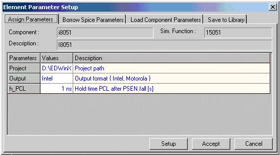
Fig.6.19
Setup
On clicking the SETUP button of Component Parameter dialog of the required model, the MMI window appears as shown in Fig.6.20.
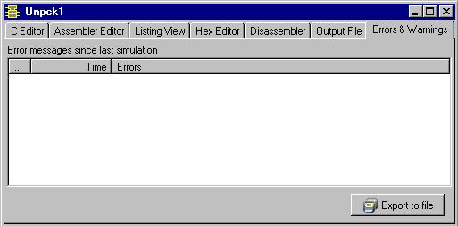
Fig.6.20
C Editor
If you intend to code the program in C, select the C Editor tab.
The different options of the C EDITOR are explained below
Clear text
The clear option helps the user to clear the context of the code editor
Import
The import option enables the user to display the Open Dialog Box to input file name and loads the text file from the disk.
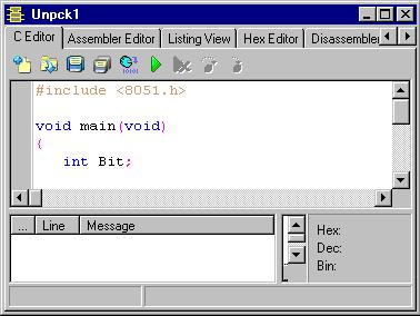
Fig.6.21
Save
The save option Generates an On Save event to notify model to save the source code in the internal file of the associated simulation component.
Export
The export option displays the On Save Dialog Box to prompt the user for output file name and saves the source code to the disk.
Compile
The compile option enables the user to Generate an On Compile event to notify model to compile the source code.
Build
The build option Generates an On Build event to notify model to compile the source code.
Start Debug
The debug option helps the user to Generate an On Debug event to notify model to debug the source code.
Stop Debug
This option allows the user to stop debugging which is associated with the generation of an On Stop debug event to notify model to stop debugging the source code.
Step Over
The option allows the user to Generate an On Step Over event to notify model to step over the being currently debugged part of code.
Trace Into
The option allows the user to Generate an On Trace Into event to notify model to trace into the being currently debugged part of code.
Assembler Editor
If you intend to code the program in Assembly Language, select the tab Assembler Editor.
Listing View
Listing view represents the listing format of assembler code.
After the compilation is done, Listing view window will present the next information i.e.
1. Real addresses of all assembler instructions used in the code.
2. Real (physical) addresses of all data in the code scope.
3. Real addresses of global variables which use the internal memory of microcontroller.
4. The initial address of stack pointer.
5. Information about used banks of registers.
You may require this information for further debugging and optimization of the source code.
Hex Editor
The Hex Editor Sheet is used to display the binary data in either Hex or ASCII formats. Also it allows to edit the binary data and provides the import and export functions.
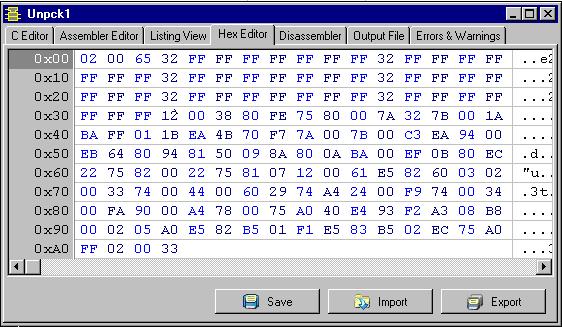
Fig.6.22
Options available in Hex Editor Sheet are:
| Import
Export Save . |
Allows to save binary data to the disk. Allows to save binary data to the disk. Generates an event to notify model that user wants the binary data to be saved in the internal file |
Disassembler
In the Disassembler window user may see the continuous address area. It reflects the instructions really loaded to the microcontroller including the library functions.
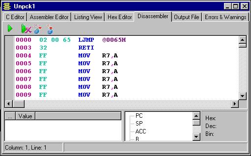
Fig.6.23
Output File
The output file generates the binary code of the program written in the C EDITOR. The output file has an option EXPORT TO FILE. The Export To File option displays the Save Dialog Box to prompt the user for output file name and saves the source code to the disk.
Errors and warnings
The Errors and Warning displays the error, warning and comment messages generated by the Mixed-mode Simulator during the Time-Domain simulation. Along with text messages (by default they are Error, Warning and Comment, though any kind of messages may be displayed), it also displays the simulation time at which the message has been generated.
There is only one function defined in Error Messages Sheet. It is Export To File. This function allows to save the displayed data to the disk.
The Error Messages Sheet doesn’t generate any events.
